3次元光学式プロファイラー 表面形状・粗さ測定
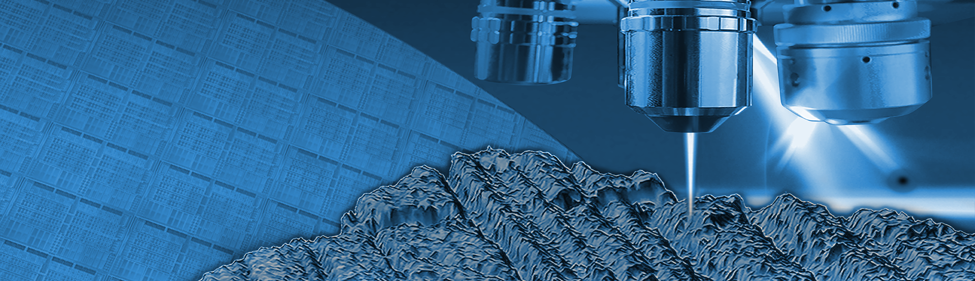
高速・非接触光学式プロファイラー(3次元白色干渉型顕微鏡/表面形状粗さ計)
ブルカーは白色干渉法を利用した表面形状・粗さ測定機のパイオニアであり、精密デバイスから車載部品等の大型試料に至るまでの幅広いサイズのサンプルに対応した 非接触3次元形状測定・分析を提供しています。最新モデルとなるContourシリーズは、10世代に渡る独自のテクノロジーの進歩の集大成であり、他の計測機器では困難な環境下での高精度で高再現性な3次元表面測定を提供しています。
38年以上にわたる光学式計測器の開発実績
1982年に世界で初めて商品化されたNCP1000(後のTOPO-2D/3Dシステム)は、当時多くの人々を驚嘆させ、その後続々と開発された製品は世界中のさまざまな業界に提供してきました。こうした実績と技術を終結させて開発したのが、Contourシリーズです。
Find the Best 3D Optical Profilometer for You


Frequently Asked Questions About 3D Optical Profilers
A 3D optical profilometer is a non-contact, non-destructive metrology system based on optical microscopy that is specifically designed for surface texture and roughness metrology in R&D and manufacturing environments. They collect data areally (over a 2D area) with a single exposure and use that data to generate 3D height maps.
Bruker's 3D optical profilometers utilize coherence scanning interferometry, also known as white light interferometry (WLI), to provide fast, accurate surface measurements over large areas to quantify a variety of surface properties. These profilers are used in engineering, research, and production process control for an extremely wide range of markets, including precision machining, medical, microelectronics, MEMS, semiconductor, solar, data-storage, automotive, aerospace, and material science.
All optical profiling techniques are 3D and quantify the topography of a surface. Optical metrology also includes techniques that are 2D and can be used to measure critical dimensions in the plane of the surface. Common systems used for 2D optical metrology include optical microscopes and scanning electron microscopes. 2D optical metrology is dependent on image contrast and sample optical properties (which may not be directly linked to topography).
Optical profilometry encompasses a wide breadth of non-contact profiling methods. These techniques all use information gained from the reflection of light off the sample surface.
Pattern projection profilometry—A light pattern is projected onto a surface, enabling analysis of the light pattern’s deformation to gain height information. This is often used for form and fit tests of mid-sized parts, such as molds, engine components, and laptops.
3D laser scanning—A laser beam is projected onto an object, and the laser’s time-of-flight before returning is used to determine the object’s position in space. This method is used to document historical objects and perform dimensional inspection of large-scale objects, such as sculptures, buildings, and car doors.
Confocal microscopy—Light is focused through a pinhole optic and 3D data is captured by scanning along the Z axis and reconstructing with only the in-focus portions of each 2D image slice in the stack. Using the pinhole optic prevents out-of-focus light from participating in image formation, limiting the depth of field. Confocal microscopy is a standard imaging technique in many biological science and some materials science applications.
Focus variation—The sharpest points (the most in-focus) from a whole 2D image stack are used to construct the 3D topography of a surface. This method is suitable for a wide range of materials and surfaces.
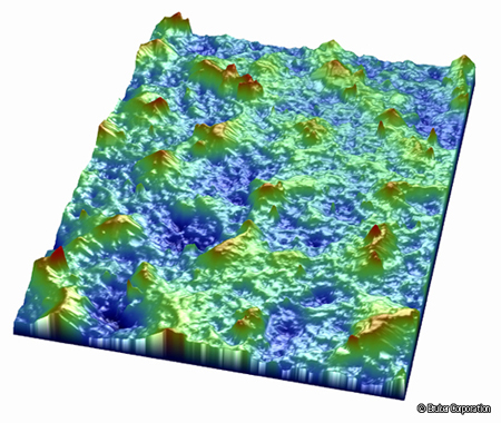
White-light interferometry—Interference patterns are generated using split and recombined light waves. The interference patterns are used to calculate surface topography with nanometer-scale resolution. WLI is used to precisely analyze sub-micron roughness of materials, such as electronics, mirrors, optics, and wafers.
White-light interferometry (WLI), also known as coherence scanning interferometry, is a non-contact optical profilometry method that takes advantage of the nature of light waves to interfere with each other constructively and destructively (i.e., wave superposition). WLI is ideal for applications where speed is critical, parts are large, samples are fragile, or there is non-uniform surface texture. These applications often show up in the research, automotive, semiconductor, biological materials, and additive manufacturing sectors, among many others.
LEARN MORE:
WLI has many advantages inherent to the technique, including:
Magnification-insensitive height resolution—WLI relies on optical interference, which is completely independent of objective lens magnification. This allows for a high vertical resolution alongside a large FOV.
High throughput—As an areal technique, WLI collects many data points at once.
No sample damage—WLI is completely non-destructive, since it is a non-contact profiling method.
Low maintenance—There are no consumables used in WLI, and self-calibrating systems further decrease maintenance requirements.
Deep-trench capabilities—WLI can profile any surface that the objective can “see”, including the bottom of high aspect ratio trenches and even sidewalls when using specialized objectives.
Using a spherical object as an example, a 2D measurement would show a circle, and a 3D measurement would show a full sphere. A 2.5D measurement is between the two, resulting in a hemisphere. Technically, optical profilers extract 2.5D measurements, though it is common to refer to the results as 3D measurements.
There are Bruker WLI systems installed in many different types of facilities, from those that experience ambient conditions to noisy fab environments and cleanrooms. Discuss your facility and requirements with our experts to find the best system for you.


3D光学プロファイラーウェビナーを見る
当社の Webinar は、ベスト プラクティスをカバーし、新製品を導入し、難しい質問に対する迅速なソリューションを提供し、新しいアプリケーション、モード、またはテクニックのアイデアを提供します。

Support

How Can We Help?
Bruker partners with our customers to solve real-world application issues. We develop next-generation technologies and help customers select the right system and accessories. This partnership continues through training and extended service, long after the tools are sold.
Our highly trained team of support engineers, application scientists and subject-matter experts are wholly dedicated to maximizing your productivity with system service and upgrades, as well as application support and training.