3D 광학 프로파일러
신속하고 비 접촉식의 3D 광학 프로파일링
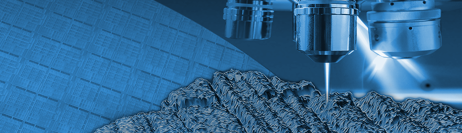
브루커는 3D 표면 측정 및 검사 솔루션의 업계 최고 제공업체로, 마이크로 MEMS에서 전체 엔진 블록에 이르는 다양한 크기의 샘플에 대해 동급 최고의 정확도를 가진 빠르고 안정적이며 사용하기 쉬운 비접촉 분석 시스템을 제공합니다. 이 시스템은 R&D, 제조 및 품질 관리 분야의 연구원과 엔지니어에게 다른 계측 시스템에서는 어려운 응용 분야 및 환경에서 정밀한 3D 표면 측정에 필요한 업계 최고의 민감도와 안정성을 제공합니다.
당사의 광학 프로파일링 계측 시스템은 10세대에 걸친 독점적인 Wyko® WLI(White Light Interferometry) 기술과 Bruker의 진보를 기반으로 전 세계 실험실 및 생산 환경에서 최첨단 R&D, QA 및 QC를 지원하는 입증된 기록을 보유하고 있습니다.
최고의 3D 광학 프로파일러 알아보기


Frequently Asked Questions About 3D Optical Profilers
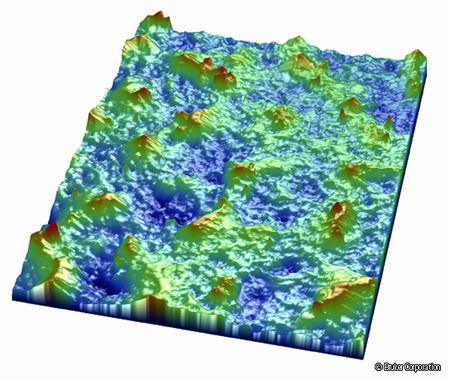
A 3D optical profilometer is a non-contact, non-destructive metrology system based on optical microscopy that is specifically designed for surface texture and roughness metrology in R&D and manufacturing environments. They collect data areally (over a 2D area) with a single exposure and use that data to generate 3D height maps.
Bruker's 3D optical profilometers utilize coherence scanning interferometry, also known as white light interferometry (WLI), to provide fast, accurate surface measurements over large areas to quantify a variety of surface properties. These profilers are used in engineering, research, and production process control for an extremely wide range of markets, including precision machining, medical, microelectronics, MEMS, semiconductor, solar, data-storage, automotive, aerospace, and material science.
All optical profiling techniques are 3D and quantify the topography of a surface. Optical metrology also includes techniques that are 2D and can be used to measure critical dimensions in the plane of the surface. Common systems used for 2D optical metrology include optical microscopes and scanning electron microscopes. 2D optical metrology is dependent on image contrast and sample optical properties (which may not be directly linked to topography).
Optical profilometry encompasses a wide breadth of non-contact profiling methods. These techniques all use information gained from the reflection of light off the sample surface.
Pattern projection profilometry—A light pattern is projected onto a surface, enabling analysis of the light pattern’s deformation to gain height information. This is often used for form and fit tests of mid-sized parts, such as molds, engine components, and laptops.
3D laser scanning—A laser beam is projected onto an object, and the laser’s time-of-flight before returning is used to determine the object’s position in space. This method is used to document historical objects and perform dimensional inspection of large-scale objects, such as sculptures, buildings, and car doors.
Confocal microscopy—Light is focused through a pinhole optic and 3D data is captured by scanning along the Z axis and reconstructing with only the in-focus portions of each 2D image slice in the stack. Using the pinhole optic prevents out-of-focus light from participating in image formation, limiting the depth of field. Confocal microscopy is a standard imaging technique in many biological science and some materials science applications.
Focus variation—The sharpest points (the most in-focus) from a whole 2D image stack are used to construct the 3D topography of a surface. This method is suitable for a wide range of materials and surfaces.
White-light interferometry—Interference patterns are generated using split and recombined light waves. The interference patterns are used to calculate surface topography with nanometer-scale resolution. WLI is used to precisely analyze sub-micron roughness of materials, such as electronics, mirrors, optics, and wafers.
White-light interferometry (WLI), also known as coherence scanning interferometry, is a non-contact optical profilometry method that takes advantage of the nature of light waves to interfere with each other constructively and destructively (i.e., wave superposition). WLI is ideal for applications where speed is critical, parts are large, samples are fragile, or there is non-uniform surface texture. These applications often show up in the research, automotive, semiconductor, biological materials, and additive manufacturing sectors, among many others.
LEARN MORE:
WLI has many advantages inherent to the technique, including:
Magnification-insensitive height resolution—WLI relies on optical interference, which is completely independent of objective lens magnification. This allows for a high vertical resolution alongside a large FOV.
High throughput—As an areal technique, WLI collects many data points at once.
No sample damage—WLI is completely non-destructive, since it is a non-contact profiling method.
Low maintenance—There are no consumables used in WLI, and self-calibrating systems further decrease maintenance requirements.
Deep-trench capabilities—WLI can profile any surface that the objective can “see”, including the bottom of high aspect ratio trenches and even sidewalls when using specialized objectives.
Using a spherical object as an example, a 2D measurement would show a circle, and a 3D measurement would show a full sphere. A 2.5D measurement is between the two, resulting in a hemisphere. Technically, optical profilers extract 2.5D measurements, though it is common to refer to the results as 3D measurements.
There are Bruker WLI systems installed in many different types of facilities, from those that experience ambient conditions to noisy fab environments and cleanrooms. Discuss your facility and requirements with our experts to find the best system for you.


당사의 3D 광학 프로파일러 웨비나 보기
당사의 웨비나는 모범 사례를 다루고, 신제품을 소개하고, 까다로운 질문에 대한 빠른 솔루션을 제공하고, 새로운 애플리케이션, 모드 또는 기술에 대한 아이디어를 제공합니다.

어떻게 도와드릴까요?

Bruker는 고객과 협력하여 실제 애플리케이션 이슈를 해결합니다. 당사는 차세대 기술을 개발하고 고객이 적합한 시스템 및 액세서리를 선택할 수 있도록 지원합니다. 이러한 협력은 장비가 판매된 후에도 오랫동안 교육 및 확장 서비스를 통해 계속됩니다.
고도로 훈련된 지원 엔지니어, 애플리케이션 과학자 및 주제 전문가 팀은 시스템 서비스 및 업그레이드뿐만 아니라 애플리케이션 지원 및 교육을 통해 생산성을 극대화하기위해 전적으로 최선을 다하고 있습니다.