Failure Analysis and Materials Characterization
Failure analysis and materials characterization groups within industrial companies are focused on solving problems to help improve process development and resolve process-related issues to help their organizations save costs and increase revenue.
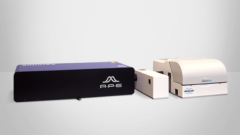
The nanoIR3-s provides a complete nanoscale FTIR, chemical imaging, and materials characterization platform. It combines two complementary nanoscale IR techniques, AFM-IR and scattering SNOM coupled with AFM-based materials property mapping. The system is productive and reliable, getting you productive data within a day. Applications include:
- Nano-organic contaminants
- LowK dielectrics
- Semiconductor materials
- Data storage media and slide
Organic nano-contaminants are a serious defectivity issue for semiconductor and data storage companies where current characterization techniques have limited capabilities. The nanoIR3 system acquires IR spectra at spatial resolutions down to 10 nm, enabling the measurement of such defects and other semiconductor materials..
The spectra generated using Bruker's patented AFM-IR technique directly correlates with traditional FTIR spectra, and are thus comparable to standard FTIR libraries. In addition to chemical analysis, nanoIR3 provides complementary mechanical, electrical, thermal, and structural property information with nanoscale spatial resolution.


