Dimension Icon
Dimension Icon
Bruker’s Dimension Icon® brings the highest levels of performance, functionality, and AFM accessibility to nanoscale researchers in science and industry. Building upon the world’s most utilized large-sample AFM platform, it is the culmination of decades of technological innovation, customer feedback, and industry-leading application flexibility. The system has been designed from top to bottom to enable the revolutionary low drift and low noise needed to achieve artifact-free images in minutes instead of hours. Dimension Icon also takes advantage of Bruker's latest milestone advancements of the NanoScope® 6 controller and ScanAsyst® Plus self-optimizing imaging software to provide enhanced intelligent algorithms and patent-pending smart functionality. These and an ever-growing catalog of hardware and software extensions deliver unmatched performance across the broadest range of applications, supporting even the most advanced and innovative research goals.
Highest Performance and Resolution
The superior resolution of the Dimension Icon, in conjunction with Bruker’s proprietary electronic scanning algorithms, provide the user with a significant improvement in measurement speed and quality. The Icon is a culmination of Bruker's industry-leading, tip-scanning AFM technology, incorporating temperature-compensating position sensors to render noise levels in the sub-angstrom range for the Z-axis, and angstroms in XY. This is extraordinary performance in a large-sample, 90-micron scan range system, surpassing the open-loop noise levels of high-resolution AFMs. The new design of the XYZ closed-loop head also delivers higher scan speed, without loss of image quality, to enable greater throughput for data collection. Bruker-exclusive PeakForce Tapping® enables Dimension Icon to routinely create the highest resolution images.
Exceptional Productivity
The Dimension family of AFMs has enabled more published data than any other large-sample AFM platform, gaining an iconic reputation in both research and industry in the process. The Icon takes the platform to a new level of excellence, providing higher performance and faster results. The software’s intuitive workflow makes performing even the most advanced AFM techniques much easier than ever before. Icon users achieve immediate high-quality results without the usual hours of expert tweaking. Every facet of the Dimension Icon — from wide-open tip and sample access to preconfigured software settings — has been specifically engineered for trouble-free operation and surprising AFM ease of use.
Maximum Flexibility
The Icon system delivers uncompromised performance, robustness, and flexibility to perform nearly every measurement at scales previously obtained by extensively customized systems. Utilizing an open-access platform, large- or multiple-sample holders, and numerous ease-of-use features, it opens up the power of AFM to research and industry alike, setting a new standard for high-quality AFM imaging and nanomanipulation.
Dimension Icon delivers flexibility without any impact to performance -- one platform, endless possibilites:
- Modify platform to correlate additional techniques
- Easily tailor your studies with open-access software and hardware -- “If it doesn’t exist, invent it”
- Complete solutions for battery, organic solar, and beyond
Contact us to discuss your measurement requirements and options for system specialization, or submit a sample run request to learn how a Bruker AFM is best suited for your applications.
Expand Your Applications with AFM Modes
With an unrivalled suite of imaging modes available, Bruker has an AFM technique for every investigation.
Built on the backbone of core imaging modes—Contact Mode and Tapping Mode—Bruker offers AFM modes that allow users to probe their samples’ electrical, magnetic, or materials properties. Bruker’s innovative new PeakForce Tapping technology represents a new core imaging paradigm that has been incorporated into several modes, providing topographic, electrical, and mechanical properties data in parallel.
Dimension Icon Data Gallery
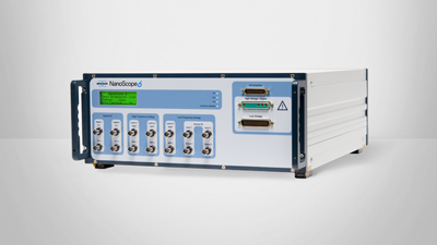
Powered by the NanoScope 6 AFM Controller
Featuring higher speeds, lower noise, and greater AFM mode flexibility, the NanoScope 6 controller allows users to harness the full potential of our high-performance Dimension and MultiMode AFM systems. This latest generation controller provides unprecedented accuracy, precision, and versatility for nanoscale surface measurements in every application.
NanoScope 6 uniquely enables Bruker AFMs to:
- Operate in more imaging modes than is possible with competing systems, including unique and advanced AFM modes that require complex control and analysis
- Collect accurate, quantitative data for nanoelectrical and nanomechanical property measurements in every application
- Optimize and customize scanning parameters to meet even the most demanding research and industry measurement requirements
- Provide ultimate ease of use with Bruker’s exclusive ScanAsyst® Plus self-optimizing imaging software with enhanced intelligent algorithms and patent-pending smart functionality (find out if your Bruker AFM is eligible for the free ScanAsyst Plus upgrade here)
Hear What Our Customers Have to Say
Bruker’s Dimension Icon is the most customizable and flexible AFM on the planet. The Dimension Icon has enabled key advances in our lab, namely the development of surface voltage microscopy and elucidation of charge transfer dynamics that are at the heart of photoanodes for solar fuel. And along the way we could always count on excellent support from Bruker’s advanced applications team.
Prof. Fengtao Fan, Group Leader, Solar Energy Research Division, and Vice Director of State Key Laboratory of Catalysis in Dalian Institute of Chemical Physics, Chinese Academy of Sciences
The Bruker Icon AFM system was installed two years ago in our clean room facility, [where it was] revealed as a unique instrument for its capability to perform low-noise and high-resolution imaging for many users, on many kind of samples and with reliable performances! ScanAsyst mode preserves the AFM probes in good condition for weeks and allows any student to be independent and to start the measurements after a short training. We are very satisfied!
Pasqualantonio Pingue, Chief Operating Officer, Laboratorio NEST, Scuola Normale Superiore, Pisa, Italy
The new multifunction atomic force microscopy of our Dimension Icon system reveals nanoscale surface characteristics and topography, such as adhesion and modulus with its ScanAsyst and PeakForce QMM. By incorporating conducting AFM and KPFM functions, interface junctions and device characteristics can both be observed, helping us to understand more detail about profile morphologies and interface states. In addition, the Icon’s high speed and reliability provides quick process checks and analysis.
Yun Yue Lin, Taiwan Semiconductor Manufacturing Company, Ltd.


