FilmTek 2000M TSV Robotic
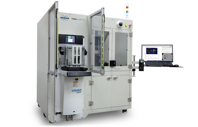
FilmTek 2000M TSV
FilmTek™ 2000M TSV 是一款采用非破坏性光学技术的全自动化量测工具,专门设计用于精确测量薄膜厚度、TSV深度、沟槽深度、关键尺寸、残留硅(residual silicon)以及总厚度变化(total thickness variation,TTV)等参数,完美适配于前道工艺与先进封装领域的发展需求。凭借其独特的数据处理算法和先进的专利硬件,该系统实现了小光斑扫描和近乎准直光束,确保了测量结果的高精度和可靠性。无论是半导体生产还是研发,FilmTek 2000M TSV都是您不可或缺的伙伴。
能够对蚀刻出的高深宽比的硅通孔(TSV)结构进行高性能测量,甚至是开口小于 1 µm 蚀刻深度高达 500 µm 的通孔结构。
测量能力
能够测量的指标如下:
TSV评估适用于直径大于1 μm,最大深度在500 μm内的通孔结构
高度或深度(Height or depth)
关键尺寸(Critical dimensions)
膜厚度(Film thickness)
System Components
Standard:
- Measure high aspect ratio TSV structures
- Measure TSV etch depth up to 500 µm
- Measure TSV structures with diameter down to 1 µm
- Patented FilmTek technology
- Fast measurement time (~1 second per point)
- TSV etch depth, bump height, critical dimension, and film thickness metrology in a single tool
- Cassette to cassette wafer handling
- Brooks or SCI automation
- 300mm, FOUP, and SMIF compatible
- SECS/GEM
典型应用

先进封装中的应用
精准掌握后道制造与封装工艺控制的每个细节
FilmTek系统提供全自动化的测量能力,包括测量实现凸点共面性(bump coplanarity)所需的厚光阻层厚度、高深宽比TSV的深度及顶部关键尺寸(CD)、键合硅片厚度或总厚度变化(TTV),以及在键合工艺中为避免非润湿开路故障而进行的薄金属氧化物层厚度测量。我们的技术确保每一步生产过程都达到高标准,帮助您提高良率,降低成本。
Typical application areas include:
- TSV metrology
- Advanced semiconductor packaging
Technical Specifications
| Measurement Function |
TSV etch depth, bump height, critical dimension, and film thickness |
|---|---|
| Wafer Handling | Brooks or Bruker |
| Substrate Size | 200 or 300 mm |
| Pattern Recognition | Cognex |
| CD Precision (1σ) | <0.2% |
| Etch Depth Precision (1σ) | <0.005% |
| Film Thickness Range | 5 nm to 350 µm (5 nm to 150 µm is standard) |
| Film Thickness Precision (1σ) | <0.005% |
| Light Source | Halogen lamp |
| Detector Type | 2048 pixel Sony linear CCD array |
| Computer | Multi-core processor with Windows™ 10 Operating System |
| Wafer Throughput | >60 WPH |
Comparison of Via Etch Depth by FilmTek 2000M TSV and SEM
| Via Diameter | SEM | FilmTek 2000M TSV |
|---|---|---|
| 5 µm | 44.5 µm | 44.3 µm |
| 10 µm | 55.5 µm | 55.5 µm |
| 15 µm | 62.0 µm | 61.8 µm |
| 20 µm | 66.5 µm | 66.8 µm |
How Can We Help?

Bruker partners with our customers to solve real-world application issues. We develop next-generation technologies and help customers select the right system and accessories. This partnership continues through training and extended service, long after the tools are sold.
Our highly trained team of support engineers, application scientists and subject-matter experts are wholly dedicated to maximizing your productivity with system service and upgrades, as well as application support and training.