
Introduction to Nanoscale Infrared Spectroscopy and Imaging with Photothermal AFM-IR
Obtain Chemical Information with Nanoscale Sensitivity and Resolution
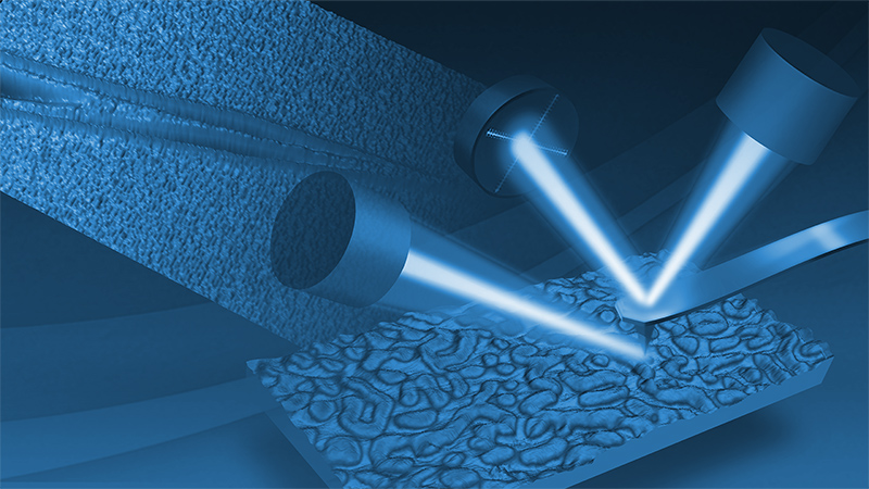
Infrared (IR) spectroscopy is a common method for the chemical characterization of organic and inorganic materials, but traditional FTIR techniques are limited in resolution and sensitivity on the order of several microns. Photothermal AFM-IR (or just AFM-IR) uses an AFM probe to detect thermal expansion of a highly localized area of material, resulting in a lateral resolution 1000x better than traditional FTIR, <1 nm detection sensitivity, and model-free interpretation.
In this webinar, Bruker experts:
- Introduce the photothermal AFM-IR technique
- Explore the simple mechanism underlying the technique
- Highlight a few of AFM-IR’s many broad applications
- Offer a demonstration of photothermal AFM-IR on the Dimension IconIR system
Webinar Summary
Infrared (IR) spectroscopy is a commonly used characterization technique for organic materials and many inorganic compounds and crystals. While powerful, it is limited by the diffraction limit to resolution on the order of several microns, and the lateral resolution is strongly dependent on the wavelength.
Photothermal AFM-IR is a novel technique which offers IR spectroscopy and imaging on materials with a lateral resolution 1000x better than traditional FTIR and <1 nm detection sensitivity with model-free interpretation. AFM-IR achieves this by using an AFM probe as the detector of photothermal expansion. This opens a variety of applications on both organic and inorganic materials where nanometer sensitivity and resolution are key.
In this webinar, Bruker experts introduce the photothermal AFM-IR technique in depth, from working principles to applications, ending with a demonstration on the Dimension IconIR system.
Find out more about the technology featured in this webinar or our other solutions for nanoscale infrared spectroscopy:
Featured Products and Technology
Speakers
Hartmut Stadler, Ph.D.
Applications Engineer, Bruker Nano GmbHHartmut Stadler works as an application scientist for Bruker Nano Surfaces and is now mainly focussed on the chemical side of AFM, including electrochemical operation and nanoscale IR techniques. His background is Physical Chemistry, with a PhD thesis in the field of biofilm characterization using macroscopic and nanoscopic methods. Since more than 25 years he operates AFMs and since more than 20 years he supports Bruker’s European AFM customers and distribution channel partners in AFM-application related questions.
Cassandra Phillips, Ph.D.
Application Scientist, BrukerCassandra did her Ph.D. at the University of Toronto exploring the photophysics of boron nitride nanotubes using scattering scanning nearfield optical microscopy (s-SNOM) and computational models. She has been working at Bruker Nano Surfaces and Metrology since September 2019 as an Applications Scientist focusing on nanoscale IR spectro-microscopy and other correlated imaging techniques realized with atomic force microscopy.
Dr. Qichi Hu, Senior Applications Scientist
Qichi is currently a Senior Staff Applications Scientist at Bruker Nano. He received a bachelor’s degree from Peking University and Ph.D. from University of British Columbia. He then did postdocs in U.S. university and national labs. Qichi has been working on nanoIR development and applications for over a decade, at Anasys and now at Bruker.
