
New Possibilities: Full Range EDS Analysis with SEM XRF
Unlock the Full Potential of your EDS Detector with SEM XRF
The addition of a micro-XRF excitation source to a Scanning Electron Microscope (SEM) equipped with an EDS detector opens up a world of new analytical possibilities.
In this webinar we will present SEM-based micro-XRF and how it can expand your systems workflow with new analytical capabilities.
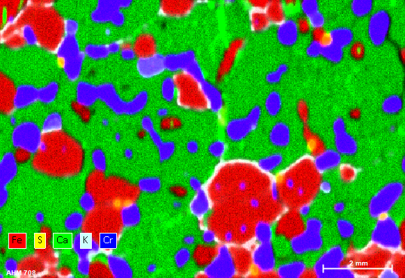
The use of a micro-XRF source allows users to overcome the limits of conventional EDS - allowing for trace element detection, layer analysis and the detection of high-energy X-ray lines. In addition, all of these benefits can also be carried out on samples with minimal preparation and that may be irregular in shape or larger than normally considered. Such possibilities turn your SEM into a Full Range EDS system.
Our micro-XRF source, XTrace 2, is equipped with a powerful 50 W micro-focus X-ray Rh tube (35 or 10 um optics), and features such as auto source retraction mode, an Aperture Management System (AMS), and Flexispot Mode, meaning it is now possible to analyze large samples at a micrometer scale.
Join us to to discover Full Range EDS and to explore how this technology can be used across a range of applications.
Who Should Attend?
- Scientists and researchers from all analytical fields interested in elemental analysis and electron microscopy.
- SEM users who want to learn about large area trace element mapping using micro x-ray fluorescence.
- SEM users who would like to analyze elements in layered samples.
- Micro-XRF on SEM users who would like to increase their analytical capabilities.


Speakers

Stephan Boehm
Product Manager - micro-XRF on SEM and WDS, Bruker Electron Microscope Analyzers

Dr. Andrew Menzies
Senior Application Scientist - Geology and Mining, Bruker AXS


Watch this Webinar On-Demand
Please enter your details below to gain on-demand access to this webinar.