FastScan Pro
Dimension FastScan Pro
The Dimension FastScan Pro delivers the highest metrology-level speed and performance of any industrial AFM available today. The system enables automated or semi-automated measurements while ensuring the utmost ease of use and the lowest cost per measurement for quality control, quality assurance, and failure analysis.
Production Versatility
FastScan Pro utilizes an open-access platform, large- or multiple-sample holders, and numerous ease-of-use features to provide flexible high-performance nanoscale metrology for industrial QA, QC, and FA applications. The system delivers automated 2-inch to 12-inch wafer measurements for semi, data storage and HB-LED. It features increased XY sample travel for full access to 200mm wafers or multiple samples in 200-mm diameter area, with optional chucks for 300-mm wafers. The system also provides the choice between a high-throughput 5-10x FastScan scanner for topography, roughness and other metrology analyses, or an Icon scanner with 90µm scan range for larger scans and high-accuracy topography performance.
Powerful Automation Software
AutoMET™ full-recipe software delivers fast, automated metrology, simple operation, and AFM adaptability for easy capture of critical-to-quality measurements needed in production. This software allows automated measurements on multiple samples or a single large sample for nanoscale characterization across multiple locations. It also provides optical and AFM image pattern recognition, tip-centering, full wafer or grid mapping support, and image-placement accuracy within tens of nanometers. Comprehensive, yet simple, recipe writing gives real-time and offline use for the advanced users.
Precise Probe-Sample Control
Unique technology enables pinpoint force to any atom on your sample. This precise probe-to-sample control permits the widest range of sample types, from soft polymers, thin films, and electrical samples to hard materials. It also provides the lowest available imaging forces and long probe tip life over hundreds of engages and data scans.
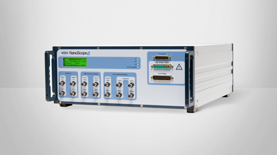
Powered by the NanoScope 6 AFM Controller
Featuring higher speeds, lower noise, and greater AFM mode flexibility, the NanoScope 6 controller allows users to harness the full potential of our high-performance Dimension and MultiMode AFM systems. This latest generation controller provides unprecedented accuracy, precision, and versatility for nanoscale surface measurements in every application.
NanoScope 6 uniquely enables Bruker AFMs to:
- Operate in more imaging modes than is possible with competing systems, including unique and advanced AFM modes that require complex control and analysis;
- Collect accurate, quantitative data for nanoelectrical and nanomechanical property measurements in every application; and
- Optimize and customize scanning parameters to meet even the most demanding research and industry measurement requirements.
Contact us to discuss your measurement requirements and options for system specialization, or submit a sample run request to learn how a Bruker AFM is best suited for your applications.
Expand Your Applications with AFM Modes
With an unrivalled suite of imaging modes available, Bruker has an AFM technique for every investigation.
Built on the backbone of core imaging modes—Contact Mode and Tapping Mode—Bruker offers AFM modes that allow users to probe their samples’ electrical, magnetic, or materials properties. Bruker’s innovative new PeakForce Tapping technology represents a new core imaging paradigm that has been incorporated into several modes, providing topographic, electrical, and mechanical properties data in parallel.

