

Thermomechanical Integrity of Thin Films and Nano-Interconnects
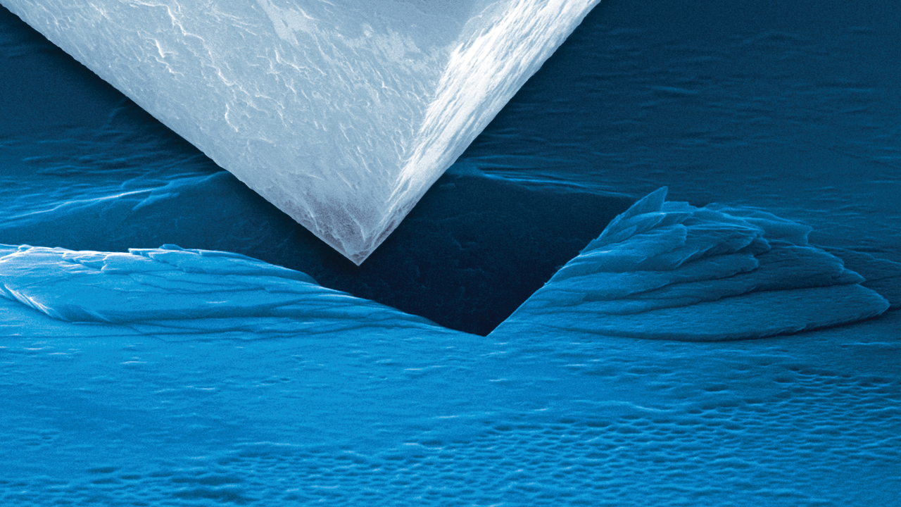
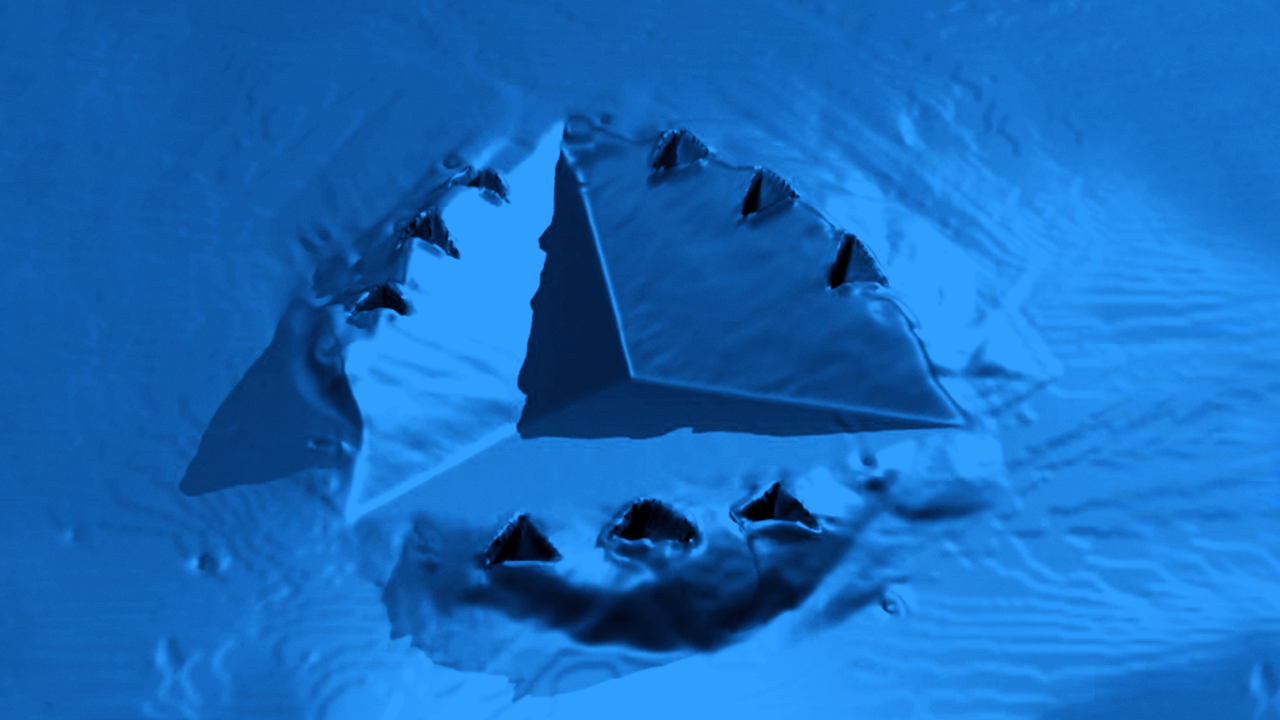
Characterize thermomechanical integrity with nanoindentation
An increasing number of material classes and complex geometries are found in integrated structures for semiconductor devices, elevating the importance of considering thermomechanical integrity to ensure optimal performance, reliability, and yield. Using nanoindentation-based characterization methods is a valuable way to understand thermomechanical integrity.
Webinar Summary
Thin films and nano-interconnects in the semiconductor industry necessarily consist of different classes of materials. As the amount of these material classes and the geometrical complexity of integrated structures increase, thermomechanical design becomes essential. Any issues with thermomechanical integrity can impact performance, yield, and reliability. In this webinar, several nanoindentation-based approaches will be demonstrated that can be used to study the thermomechanical integrity of thin films and nano-interconnects for semiconductor applications.
Find out more about the technology featured in this webinar or our other solutions for nanomechanical testing:
Featured Products and Technology

Guest Speaker

Dr. Kris Vanstreels
Researcher, IMECKris Vanstreels received the Master of Science degree in Physics from KU Leuven in 2001 and the PhD degree in Physics from UHasselt in 2007. From 2001 to 2007, he was working as a researcher at the institute of materials research of UHasselt, where he was involved in the physical characterization of different materials systems and the development of high resolution in-situ measurement techniques. From November 2007 on he joined the Reliability and Modeling group of IMEC in Belgium as a researcher. His main research activities are focused on mechanical characterization and reliability of back-end-of-line stacks and 3D stacked-ICs.