
Bruker’s 2024 AFM Probes Webinar
Discover the keys to AFM success, according to our experts
Hear directly from Bruker’s applications and demonstration-lab atomic force microscopy experts, as they answer these questions:
- What is your favorite AFM probe and why?
- What applications- and technique-specific tips and tricks do you have?
Webinar Summary
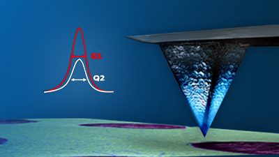
Watch this on-demand webinar, where we interview various Bruker application engineers worldwide on what their favorite, go-to probe is and why. Wealso virtually visit various demonstration labs to get tips and tricks from dedicated bioAFM, nanoIR, and automated AFM application engineers. You'll definitely discover some new probe types and maybe new ways to use legacy types!
Find out more about the technology featured in this webinar or our other solutions for AFM:
Related Resources
Speaker

Ian Armstrong, Ph.D., Senior Manager AFM Probes, Bruker
Ian Armstrong has worked at Bruker for over 16 years in various roles from applications to product management. He is currently senior manager of Bruker's AFM probes business unit.

Ravi Chintala, Ph.D.
Application Scientist, Bruker Nano SurfacesRavi Chintala is currently working as Application Scientist at Bruker Nano Surfaces. Ravi Chintala, has more than 10 years of research experience on scanning probe microscopy, focusing specifically on various electrical SPM techniques. Before starting his career as an Application Scientist at PrimeNano,Inc., Dr. Chintala was a postdoctoral fellow at Lawrence Berkeley National Laboratory investigating nanoscale charge carrier dynamics of solar cells using KPFM. Dr. Chintala has obtained his PhD from IMEC, (Belgium) and MS from Michigan Technological University (Houghton, MI).

Sean Hand,
Senior Staff Applications Scientist, BrukerSean Hand is a Senior Staff Applications Scientist with Bruker's Automated AFM group focused on the application of AFM to semiconductor manufacturing. Sean has an M.S. in physics from the University of Vermont where he focused on Atomic Force Microscopy of lipid bilayers for transdermal drug delivery. Sean has over 25 years of experience in AFM for semiconductor manufacturing and has co-authored over 20 papers and owns several patents related to Automated AFM in semiconductor manufacturing.

Peter De Wolf, Ph.D., Director of Technology & Application Development
Peter De Wolf is director for AFM technology & application development at Bruker Nano Surfaces, covering all applications related to Scanning Probe Microscopy (SPM). He obtained his PhD from IMEC, Belgium on the development of new SPM methods for 2D carrier profiling in semiconductors and has more than 25 years of experience on SPM. He is the author and co-author of over 30 publications related to electrical characterization using SPM. He also owns several SPM patents, and developed several new SPM modes for electrical characterization.

Ming Ye, Ph.D., Applications Scientist, Bruker
Ming Ye earned his Ph.D. in chemistry from the Chinese Academy of Sciences and has more than 15 years of BioAFM experience.

Alexander Dulebo, Ph.D.
Bio Sales Application Engineer, Bruker

Mickael Febvre, Ph.D.
Application Manager, Bruker EMEA