
Advanced Material Characterization in SEM with EBSD Analysis
Material Analysis with Electron Backscatter Diffraction in the Electron Microscope
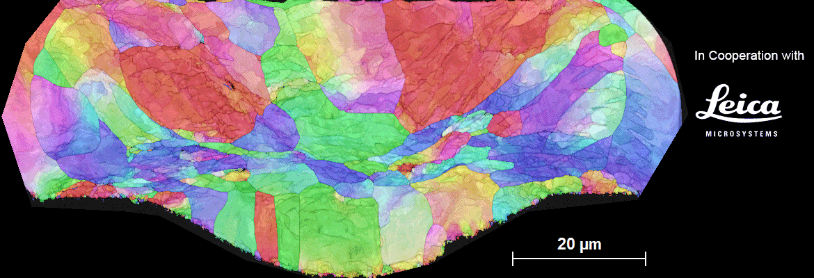
Electron Backscatter Diffraction (EBSD) is a well-established scanning electron microscope (SEM) based technique used for material characterization. Microstructural organization (crystallographic information) of the material is assessed by analyzing diffraction patterns to determine the crystal orientation, characterize grain boundaries, provide information about the local crystalline status, as well as identify and distinguish phases when combined with EDS measurement.
Good specimen preparation is key to analytical electron microscopy techniques such as EBSD, since electron diffraction is generated within a few tens of nanometers of the sample surface.
In this webinar, we present advanced yet straightforward sample preparation solutions for semiconductor and material research applications. Corresponding EBSD measurements are achieved successfully, allowing the complete microstructural characterization of challenging materials. We also demonstrate the preparation of electron transparent sample required for analyzing ultra-fine-grained material by Transmission Kikuchi Diffraction (TKD) technique.
This 45 min webinar will conclude with a 15-minute live Q&A session where our experts will answer your questions.
Who Should Attend
- SEM microscopists interested in advanced analytical techniques for material characterization
- EBSD users of all levels
Speakers
Dr. Laurie Palasse
Global Application Manager, Bruker Electron Microscope Analyzers
Ms. Angela Hu
Sales & Applications Specialist, Nanotechnology, Leica Microsystems (SEA)
Watch this Webinar On-Demand
Please enter your details below to gain on-demand access to this webinar.


