

Resonance Enhanced Force Volume AFM-IR: A Powerful New Technique for Nanoscale IR Characterization
Learn about the Latest Nanoscale IR Characterization Technique:
REFV AFM-IR
Highlights of this webinar include:
- Introduction to the REFV AFM-IR technique
- Outline of performing simultaneous multimodal imaging and spectroscopy
- Introduction to new mechanical tracking methods
- New applications offered by REFV AFM-IR
- Demonstration of the technique
- Q&A session - don’t miss the opportunity to pose your questions to our NanoIR experts
Webinar Summary
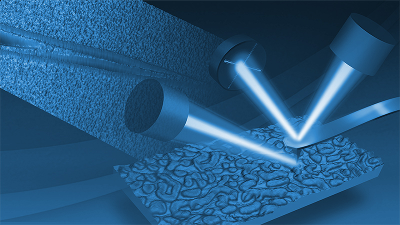
Nanoscale infrared microscopy enables label-free, chemical imaging and spectroscopy at the nanometer scale by combining atomic force microscopy (AFM) with infrared radiation. Over the years, different AFM-IR modes have been developed: The original photothermal-induced resonance enhanced mode and surface sensitive AFM-IR are based on contact mode, while Tapping AFM-IR is built on tapping mode. All of these nanoIR variations, however, have the inherent advantages and limitations of their respective AFM base mode.
Resonance Enhanced Force Volume (REFV) AFM-IR is a novel approach that relies on off-resonance tapping to simultaneously capture nanomechanical and nanochemical properties and deliver previously inaccessible insights into material properties.
Find out more about the technology featured in this webinar or our other solutions for nanoscale IR characterization:
Featured Products and Technology

Speakers

Peter De Wolf, Ph.D., Director of Technology & Application Development
Peter De Wolf is director for AFM technology & application development at Bruker Nano Surfaces, covering all applications related to Scanning Probe Microscopy (SPM). He obtained his PhD from IMEC, Belgium on the development of new SPM methods for 2D carrier profiling in semiconductors and has more than 25 years of experience on SPM. He is the author and co-author of over 30 publications related to electrical characterization using SPM. He also owns several SPM patents, and developed several new SPM modes for electrical characterization.

Cassandra Phillips, Ph.D.
Application Scientist, BrukerCassandra did her Ph.D. at the University of Toronto exploring the photophysics of boron nitride nanotubes using scattering scanning nearfield optical microscopy (s-SNOM) and computational models. She has been working at Bruker Nano Surfaces and Metrology since September 2019 as an Applications Scientist focusing on nanoscale IR spectro-microscopy and other correlated imaging techniques realized with atomic force microscopy.

Dr. Qichi Hu, Senior Applications Scientist
Qichi is currently a Senior Staff Applications Scientist at Bruker Nano. He received a bachelor’s degree from Peking University and Ph.D. from University of British Columbia. He then did postdocs in U.S. university and national labs. Qichi has been working on nanoIR development and applications for over a decade, at Anasys and now at Bruker.