Application Note: High-Performance Nanoscale IR Spectroscopy and Imaging with Dimension IconIR
Enabling Highest-Performance Chemical Identification at the Nanoscale
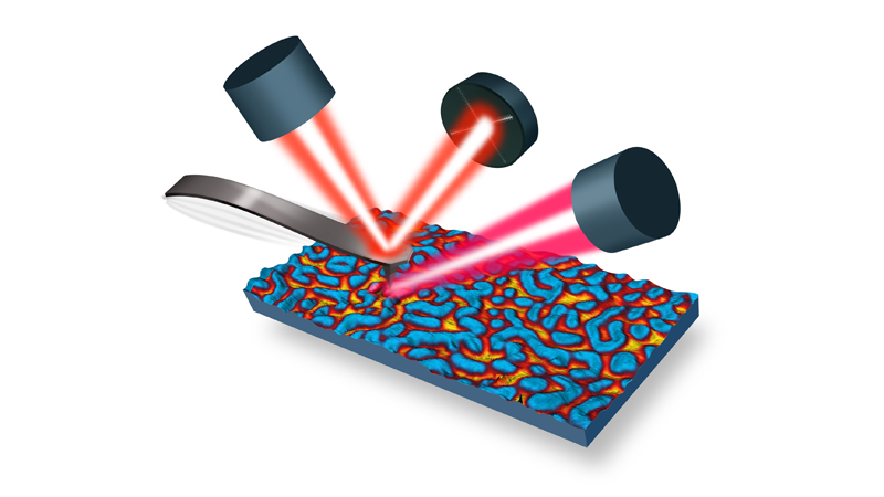
Photothermal atomic force microscope infrared spectroscopy (AFM-IR) enables chemical identification at the nanoscale. The Dimension IconIR™ platform currently has the highest performance in the world for AFM-IR measurements, leveraging advancements in IR laser sources, system designs, and operating modes to improve detection sensitivity, lateral resolution, surface sensitivity, measurement speed, and mechanical artifact correction.
This application note examines the key factors governing photothermal AFM-IR performance, with examples showing the achievement of sub-nanometer detection sensitivity, high lateral resolution (<2 nm), controlled probing depth, high throughput for spectroscopy and imaging, and removal of mechanically induced artifacts.
Readers can expect to:
- Gain an understanding of the comprehensive definition of “high-performance”, as it relates to AFM-IR capabilities.
- See examples for each performance category, showcasing real samples and data.
- Connect distinct advances with their direct impact on AFM-IR instrument performance.
KEYWORDS: Nanoscale IR Spectroscopy; AFM-IR; Photothermal AFM-IR; Nanochemistry; nanoIR; Chemical Identification; Application Note; Tapping AFM-IR; Resonance Enhanced AFM-IR; Surface Sensitive AFM-IR; Dimension IconIR

Introduction
Photothermal atomic force microscope infrared spectroscopy (AFM-IR) enables chemical identification on the nanoscale. This technique was first developed by Alexandre Dazzi in 20051 and the first-generation nanoIR system was commercialized in 2010. Since then, significant advancements have been made in the IR laser sources, system designs, and operating modes to improve detection sensitivity, lateral resolution, surface sensitivity, measurement speed, and mechanical artifact correction.2-5 Harnessing these critical improvements, the Dimension IconIR™ platform currently has the highest performance in the world for AFM-IR measurements, resulting in new, previously inaccessible insights. In this application note, the key factors governing photothermal AFM-IR performance will be examined, with examples showing the achievement of sub-nanometer detection sensitivity, high lateral resolution (<2 nm), controlled probing depth, high throughput for spectroscopy and imaging, and removal of mechanically induced artifacts.
Detection Sensitivity (<1 nm)
Superior engineering and system design, including knowledge of the factors governing core atomic force microscope (AFM) performance, has led to the high sensitivity of Bruker’s photothermal AFM-IR. This has been demonstrated through the measurement of various thin samples, including self-assembled monolayers and single protein molecules.6
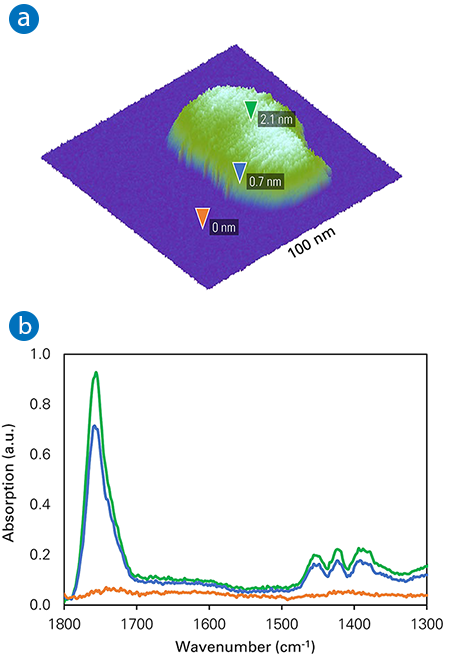
Figure 1 shows the AFM-IR data obtained from a thin polylactic acid (PLA) sample on a mica substrate. AFM-IR spectra were acquired from two locations on the PLA sample with thicknesses of 0.7 and 2.1 nm, respectively. A third spectrum was collected from a single location on the substrate for comparative purposes. The three locations are identified by colored markers corresponding to the AFM-IR spectra of the same color.
In contrast to the featureless baseline observed in the substrate spectrum, the PLA material exhibited distinct IR bands, including the carbonyl stretching band at 1750 cm-1 and C-H bending bands near 1400 cm-1. The inset of the figure displays a 3D image overlaying the topography with the IR absorption signal recorded at 1750 cm-1, highlighting the excellent contrast between the PLA material and the mica substrate. Note that mica is a non-enhancing substrate. Previous monolayer measurements have been done on metallic substrates which enhance the electric field of the IR beam and improve the AFM-IR measurement sensitivity.
The exceptional sensitivity of the photothermal AFM-IR technique has also facilitated the characterization of inorganic materials with extremely small thermal expansion coefficients. A notable example involves the application of Tapping AFM-IR to investigate the surface plasmonic polariton (SPP) in a monolayer of graphene on a silicon substrate.7 In this study, a fringe pattern attributed to the propagation and interference of the SPP wave was observed at the edge of the graphene wedge. This observation aligns with findings from previous studies utilizing scattering-type scanning near-field optical microscopy (s-SNOM).8
Spatial Resolution (<2 nm)
The primary advantage of photothermal AFM-IR over traditional bulk Fourier transform infrared spectroscopy (FTIR) lies in its nanoscale spatial resolution. The achievable limit of spatial resolution in AFM-IR has progressively advanced from approximately 50 nm with an IR laser source at a fixed pulse rate of 1 kHz, to about 20 nm in Resonance Enhanced mode while utilizing a quantum cascade laser (QCL) with a tunable pulse rate of up to 3 MHz, then to better than 10 nm in Tapping AFM-IR and Surface Sensitive modes.
The Dimension IconIR system has consistently demonstrated better than 10 nm spatial resolution for a variety of samples. Figure 2 shows a Tapping AFM-IR image of an organic self-assembled monolayer (octadecyl 4’-octadecyloxy-4-biphenylcarboxyloate, EsterOC18) onhighly oriented pyrolytic graphite (HOPG), another non-enhancing substrate. The molecule has a phenyl core and two side aliphatic chains (Figure 2d). The monolayer has a periodicity of 5.6 nm, and a thickness of 0.8 nm.9
One AFM-IR image was recorded at 1460 cm-1, corresponding to the C-H bending of the side chains (Figure 2a). The image revealed a periodic pattern of stronger and weaker signals, with the former attributed to the side chains and the latter to the phenyl core. To confirm genuine chemical contrast in this IR image, a second image (Figure 2b) was recorded at 1600 cm-1, a wavelength with no absorption, resulting in no observable contrast.
A profile analysis of the IR image at 1460 cm-1 demonstrated periodic fluctuations in signal intensity, aligning with the molecular size of EsterOC18 (Figure 2c). By measuring the distance between 10% and 90% of the maximum IR signal intensity, a spatial resolution of <2 nm was consistently obtained at multiple rising or falling edges of the profile curve. This high spatial resolution is attributed to several factors, including: selection of a sample with appropriate molecular size and IR absorptions, the heterodyne detection scheme employed in Tapping AFM-IR, a high laser pulse rate of around 1.5 MHz, and enhancement of the IR beam's electric field at the AFM tip apex.
The stability and low-noise performance of the Dimension IconIR system is also critical to the success of measurements at these small scan sizes. For example, no distortion was observed in the parallel self-aligned molecules in these images, highlighting the minimal system drift, which is typically smaller than 0.2 nm/min.

Surface Sensitivity
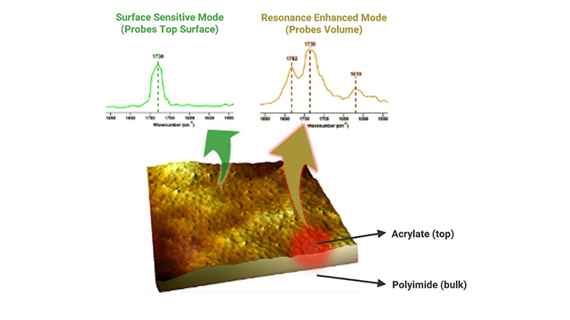
Similar to advancements in lateral resolution, progress has also been made in the precision for characterizing and controlling vertical probing depth. The Dimension IconIR system can be equipped with a variety of AFM-IR modes, each complementing the others in terms of desired probing depth. Since diligent calibration of probing depth is crucial for surface sensitivity claims, Bruker and collaborators have conducted systematic investigations into the probing depth of each AFM-IR mode, using carefully designed samples, such as a thin polymer wedge on a second polymer bulk sample.
By strategically employing a combination of different AFM-IR modes and settings, it becomes possible to analyze materials at various depths within the sample. The Resonance Enhanced mode has a typical probing depth of 50 nm or more, up to microns. Detection of a higher resonance of the AFM probe (by using a higher laser pulse rate) yields a smaller probing depth. The Tapping AFM-IR mode typically achieves a probing depth of 30–100 nm, while the Surface Sensitive mode detects the top layer of 10–50 nm for a typical polymeric sample.4
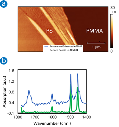
Figure 3 presents the topography image and AFM-IR spectra collected from a polymer blend sample—a polymethyl methacrylate (PMMA) bulk material with a thin polystyrene (PS) film on top in certain areas (Figure 3a). AFM-IR spectra (Figure 3b) were collected from a location with a 30 nm thick PS layer using two different modes. The spectrum in Resonance Enhanced mode exhibited absorption from both the top PS layer (1452, 1492, and 1600 cm-1) and bulk PMMA (1736 cm-1). In contrast, the spectrum in Surface Sensitive mode showed absorption solely from the top PS layer, without contribution from the bulk PMMA. The result indicated that the Surface Sensitive mode has a probing depth of <30 nm in this specific measurement.
High Scan Rate for IR Imaging
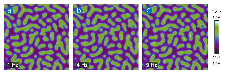
With commercial AFM-IR setups, IR imaging was typically conducted at a line rate of 1 Hz or lower. Built on the Icon platform with enhanced AFM performance, the Dimension IconIR system is capable of collecting IR absorption images at higher scan rates, leading to a significant increase in the throughput of AFM-IR measurements.
Figure 4 shows the Tapping AFM-IR images of a PS-PMMA block copolymer sample on a silicon substrate. The images were recorded at 1730 cm-1, with line rates of 1, 4, and 9 Hz. The PS-PMMA block copolymer has a relatively smooth sample surface, and a small pitch size of about 40 nm. Distinct PMMA domains with a stronger signal and the PS matrix with a weaker signal were clearly resolved In the IR images. No degradation of signal/noise or spatial resolution was observed at higher imaging rates, and at the line rate of 9 Hz, a 256x256 pixel full IR image was acquired in less than 30 seconds.
In the case of a rougher sample, such as a polymer sample containing PMMA beads embedded in the epoxy matrix, with a surface roughness on the order of a couple of hundred nanometers, a line rate of ~3 Hz was evaluated for a large scan area of 10x10 µm. At this scan rate, a reasonable signal-to-noise ratio was shown in the Tapping AFM-IR images.
To increase scan rate even further, the Dimension IconIR software offers a “bidirectional” IR imaging feature that allows the system to scan trace and retrace alternatively for adjacent lines. Enabling this feature effectively doubles the scan rate without compromising the signal-to-noise ratio of the IR images.
Hyperspectral Imaging
With advancements in the Dimension IconIR system significantly increasing imaging speeds, hyperspectral imaging (where a spectrum is collected at each pixel in an image) has become a routine measurement mode. The sweeping speed of the IR laser source has undergone steady improvement. Enhanced communication efficiency between the controller and the IR laser sources has reduced the time gap between two spectroscopic measurements. Currently one can acquire an AFM-IR spectrum in approximately 1 second in the hyperspectral imaging mode.
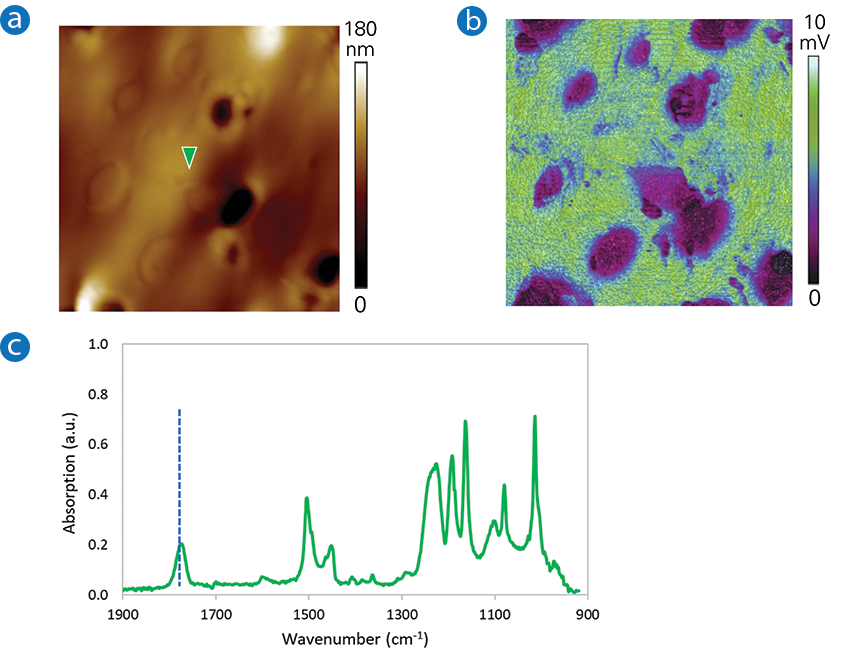
Figure 5 shows the hyperspectral imaging results of a sample containing polycarbonate (PC) and acrylonitrile butadiene styrene (ABS). An array of 64x64 (4096 total) AFM-IR spectra were collected over an area of 3x3 µm2. A representative spectrum, extracted from the location labelled by a green mark in the topography image, identifies the local material as PC.
Once the hyperspectral array is completed, an IR absorption image at any wavenumber within the spectral range can be generated by defining and moving a cursor in the AFM-IR spectrum. Figure 5 illustrates an IR absorption map at 1775 cm-1, corresponding to the carbonyl absorption band of PC. The IR map clearly displays the distributions of the PC component with a stronger signal and the ABS component with a weaker signal.
An essential factor in hyperspectral imaging is preventing sample drift over the extended measurement durations. The Dimension IconIR system has superior performance in this regard, with a typical sample drift rate smaller than 0.2 nm/min. The system’s fast spectral sweep and minimal thermal drift allow for efficient collection of a hyperspectral dataset within a reasonable timeframe, free from distortion. This characteristic establishes a robust correlation between the AFM-IR spectrum and the sample location, ultimately enhancing the reliability and accuracy of hyperspectral imaging results.
Mechanical Compensation and PLL
The mechanical stiffness of samples can influence the overall signal in AFM-IR measurements, making it crucial to distinguish between mechanical artifacts and genuine IR absorption signals. In this aspect, the Dimension IconIR system is well-equipped, providing researchers with the confidence to accurately discern and interpret their measurements.
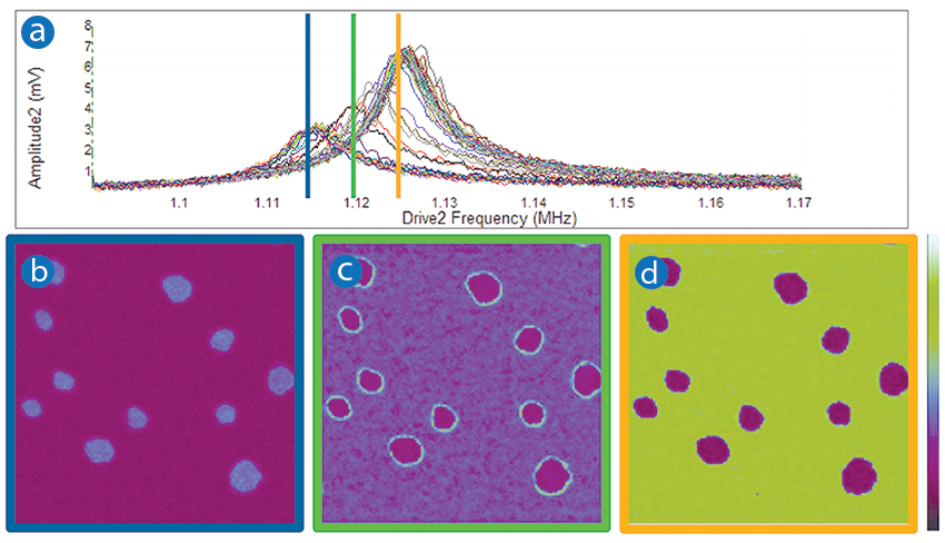
Figure 6 shows the results from polymer blend sample, with small domains of one polymer embedded in the matrix of a second polymer. AFM-IR signal was recorded in the Resonance Enhanced mode at various points along a single scan line. The signal is plotted as a function of the laser pulse rate, tuned near a contact resonance frequency of the cantilever at 1.12 MHz (Figure 6a). The resonance frequency undergoes shifts due to AFM tip interactions with a heterogeneous sample, resulting in a maximum AFM-IR signal at different laser pulse rates.
Observing the data, it becomes evident that maintaining a fixed laser pulse rate leads to a decrease in contrast in the IR absorption image (Figure 6b-d) as the laser pulse rate shifts from the position indicated by the orange cursor to that indicated by the green cursor. The contrast is even inverted as the laser pulse rate is moved to the position indicated by the blue cursor. This type of mechanical-induced shifts is present in all AFM-IR modes, and underscores the importance of removing mechanical artifacts from AFM-IR measurements.
To address variations in sample mechanical stiffness, the Dimension IconIR system incorporates a phase-locked loop (PLL) scheme for every AFM-IR mode. Specifically, the Resonance Enhanced mode features a single PLL to track the probe contact resonance frequency. Tapping AFM-IR and the Surface Sensitive mode employ a dual PLL scheme, with one PLL tracking the probe driving frequency and a second PLL tracking the probe detection frequency. The dual PLL allows separate and accurate tracking of the driving frequency and detection frequency, ensuring a more stable driving amplitude during the measurement and maximizing the AFM-IR signal. In addition to mechanical compensation, the probe frequency channels can be acquired during the AFM-IR measurements, providing complimentary information on the sample mechanical properties.
The PLL scheme incorporated into the Dimension IconIR system proves to be robust and effective, particularly when measuring samples with relatively large mechanical variations. This capability has been demonstrated through successful AFM-IR measurements on a meteorite sample featuring both organic and inorganic components.10 The substantial mechanical differences between these components had posed challenges in previous AFM-IR measurements, but the powerful PLL scheme in the Dimension IconIR system effectively addressed and compensated for such variations, ensuring accurate and reliable results.
Dimension IconIR Redefines High-Performance AFM-IR
As demonstrated here, Bruker’s Dimension IconIR excels at achieving high sensitivity, high spatial resolution, controlled probing depth, high throughput, and excellent mechanical compensation. It currently stands as the platform with the highest performance in the world for AFM-IR measurements, and continues to advance with the development of new capabilities.
Conclusions
Authors
- Qichi Hu, Ph.D., Senior Staff Applications Scientist, Bruker (qichi.hu@bruker.com)
- Jinhee Kim, Ph.D., Applications Scientist, Bruker (jin_hee.kim@bruker.com)
- Martin Wagner, Ph.D., Senior Staff Scientist, Bruker (martin.wagner@bruker.com)
- Chunzeng Li, Ph.D., Senior Engineer Development Application, Bruker (chunzeng.li@bruker.com)
- Cassandra Phillips, Ph.D., Product Manager Nanoscale IR Spectroscopy, Bruker (cassandra.phillips@bruker.com)
- Peter De Wolf, Ph.D., Senior Director of Technology and Application Development, Bruker (peter.dewolf@bruker.com)
References
- Dazzi, A., Prazeres, R., Glotin, F., Ortega, J. M., Opt. Lett. 30, 2388-2390 (2005).DOI: 10.1364/OL.30.002388
- Lu, F., Jin, M., Belkin, M. A., Nat. Photon. 8, 307-312 (2014). DOI: 10.1038/nphoton.2013.373
- Mathurin, J., Pancani, E., Deniset-Besseau, A. et al., Analyst 143, 5940-5949 (2018).DOI: 10.1039/C8AN01239C
- International Patent WO2020049053; United States Patent US 11,215,637 B2.
- Ramer, G., Reisenbauer, F., Steindl, B. et al., Appl. Spectrosc. 71, 2013-2020 (2017).DOI: 10.1177/0003702817695290
- Ruggeri F.S., Mannini, B., Schmid, R. et al., Nat. Commun. 11, 2945 (2020).DOI: 10.1038/s41467-020-16728-1
- Menges, F., Yang, H., Berwerger, S. et al., APL Photonics 6, 041301 (2021). DOI: 10.1063/5.0044738
- Gerber, J.A., Berweger, S., O’Callahan, B.T., Raschke, M.B., Phys. Rev. Lett. 113, 055502 (2014).DOI: 10.1103/PhysRevLett.113.055502
- Hamadeh, A., Palmino, F., Mathurin, J. et al., Commun. Chem. 6:246 (2023).DOI: 10.1038/s42004-023-01036-8
- Yabuta, H., Cody, G.D., Engrand, C. et al., Science 379, eabn9057 (2023).DOI: 10.1126/science.abn9057
©2024 Bruker Corporation. Dimension IconIR is a trademark of Bruker Corporation. All other trademarks are the property of their respective companies. All rights reserved. AN206, Rev. A0.