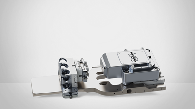

Small-Scale Mechanical Testing in the Scanning Electron Microscope (SEM)
Discover the capabilities of Hysitron SEM PicoIndenters
The coupling of scanning electron microscopy and nanoscale mechanical testing allows researchers to precisely probe sample surfaces while observing material deformation in real-time.
In this webinar, a Bruker expert on the Hysitron PicoIndenter product line describes the instruments’ capabilities, including:
- Standard nanoindentation
- Beam bending
- Pillar compression
- Heated testing
- Tribological testing
Webinar Summary
This webinar provides an overview of Hysitron's PicoIndenter product line for performing small-scale mechanical testing inside the scanning electron microscope (SEM). Joe Lefebvre, the product manager, begins by introducing the motivation for using nanoindentation and other techniques at the small scale.
He describes how the PicoIndenter instruments work using a three-plate capacitive transducer to measure force and displacement. Lefebvre then shows various examples of tests that could be performed, including standard nanoindentation, targeted indentation of specific phases, beam bending, pillar compression, and more. Some advanced applications are also covered, such as heating samples during testing, using additional tilt and rotation stages, and performing scratch and tribology tests.
At the end, audience questions address sample compatibility concerns, non-conductive sample coating effects, and the ability to combine nanoindentation with EBSD or EDS characterization. In summary, the webinar provides a thorough overview of Hysitron's capabilities for nanomechanical testing integrated with SEM imaging.
Find out more about the technology featured in this webinar or our other solutions for Small-Scale Mechanical Testing:
Featured Products and Technology
Speaker
Joseph Lefebvre
Product Line Manager of Hysitron Microscopy Products at Bruker


