ZH
My Bruker
联系我们
产品与解决方案
应用
服务与支持
新闻和活动
关于我们
职业
请至少输入2个字符 (您当前输入的是1个字符) 。
Languages
Deutsch
English
Español
Français
Italiano
Polski
Português
Русский
中文
日本語
한국어
▶ Watch On-Demand | 50 Minutes
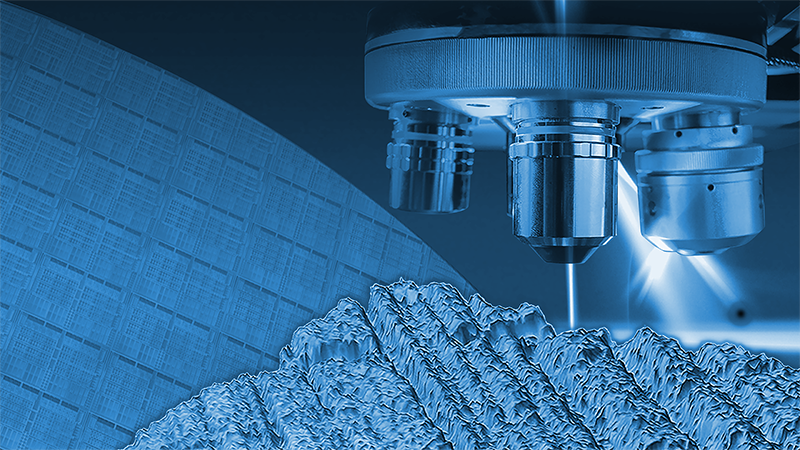
Accelerating Semiconductor Processes Control with Advanced 3D Optical Metrology
Learn how recent advances in 3D Optical Metrology accelerate in-line quality control for both front- and back-end processes
Presented by Samuel Lesko, Ph.D., Dir. of Technology and Apps Development, Bruker Nano Surfaces & Metrology (December 17, 2019)
PRESENTATION HIGHLIGHTS:
[00:03:46]
Review of non-contact interferometric profiler components, modes, and attributes
[00:16:15]
Front-end (FEOL) quality control solutions for semiconductor manufacturing
[00:29:45]
Back-end (BEOL) quality control solutions for semiconductor manufacturing
LIVE AUDIENCE Q&A:
[00:46:43]
What lateral resolution can you expect when scanning RDL layers?
[00:47:53]
What is the layer thickness limit for characterization of transparent layers?
[00:49:06]
How do you cope with different refractive indexes or oxide thicknesses for CMP measurements of films?
Featured Products and Technology
3D Optical Profilers
Non-contact 3D surface measurement, inspection, and analysis
阅读更多
REQUEST MORE INFORMATION
3D Surface Measurements
The history, development, advantages and applications
阅读更多
REQUEST MORE INFORMATION
Related Webinars
On-Demand Session • 55 Minutes
Solving Challenges in Defect Inspection of Advanced Optics
Gain new insight into the inspection process for advanced optical materials, including strategies for defect detection, ranking, and mapping for complex geographies and large and aspheric optics.
On-Demand Session • 1 Hr 5 Minutes
Qualifying Surface and Device Performance Through Roughness Quantification
Learn how to measure micro-roughness in accordance with the ISO 25178 norm to assess device performance and efficiency and, ultimately, improve product and process design.
On Demand • 2 Hrs
Surface Characterization of Semiconductors: An Overview, from Topography to Advanced Physical Properties
Watch exclusive expert lectures and live demonstrations of Bruker’s high-performance metrology technology and the latest techniques for the nanometer-scale surface characterization of semiconductor materials and devices.
RETURN TO SESSION OVERVIEW