Characterization of Thin Dielectric Films with Atomic Force Microscopy (AFM)
Learn how AFM can be applied to measure and quantify the properties of dielectric film.
This webinar focuses on the various possibilities offered by Bruker AFM modes to measure and quantify the properties of dielectric films. Each method is illustrated with case studies, and two short live demonstrations were held on a Bruker Dimension Icon to portray the practical implementation and operation of two of the electrical characterization modes.
Investigate Characterization of Thin Dielectric Thin Films with AFM
The properties of dielectric materials play a crucial role in their suitability for a range of high-performance applications in the semiconductor and microelectronic industries, and as insulation and packaging materials.
In this webinar, the presenters illustrate how AFM can be applied to measure and quantify the properties of dielectric films using:
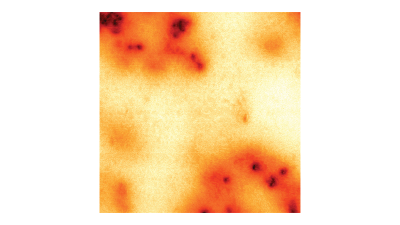
- Nanometer-scale topography mapping and accurate measurement of roughness and step height. Practical aspects, such as tip and mode selection and how to overcome ESD effects, are addressed.
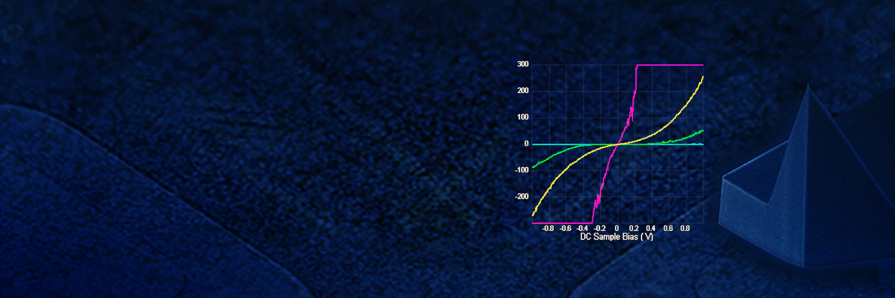
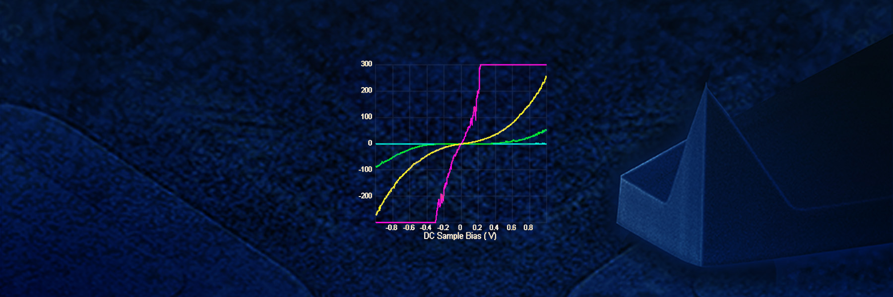
- Conductive AFM (C-AFM) and Tunneling-AFM (TUNA): Nanoscale electrical characterization can be applied to study tunnel currents through dielectrics by current imaging and current-voltage point spectroscopy. These data provide insight into dielectric properties such as film thickness uniformity, the presence of defects, and breakdown behavior (reversible & irreversible). The method also extends to time-dependent breakdown measurements.
- Electric field Microscopy (EFM) and Kelvin Probe Force Microscopy (KPFM): Study charge distribution and capacitance related effects.
- Scanning Microwave Impedance Microscopy (sMIM): The tip/sample capacitance is measured with high spatial resolution and sensitivity to study variations in the dielectric thickness and dielectric constant. The capacitance imaging capability is augmented with C-V spectroscopy capability, providing further insights into the local dielectric properties.
Each method was illustrated with case studies, and two short live demonstrations were held on a Bruker Dimension Icon to illustrate the practical implementation and operation of two of the electrical characterization modes.
Find out more about the technology featured in this webinar or our other solutions for AFM:
Featured Products and Technology


Speaker(s)

Peter De Wolf, Ph.D., Director of Technology & Application Development
Peter De Wolf is director for AFM technology & application development at Bruker Nano Surfaces, covering all applications related to Scanning Probe Microscopy (SPM). He obtained his PhD from IMEC, Belgium on the development of new SPM methods for 2D carrier profiling in semiconductors and has more than 25 years of experience on SPM. He is the author and co-author of over 30 publications related to electrical characterization using SPM. He also owns several SPM patents, and developed several new SPM modes for electrical characterization.

Mickael Febvre, Ph.D.
Application Manager, Bruker EMEA

Andrea Slade, Ph.D., Product Manager, Materials AFM, Bruker Nano Surfaces & Metrology
Dr. Andrea Slade received her Ph.D. in Biochemistry / Biomedical Engineering from the University of Toronto on the integration of AFM with optical microscopy for the study of biological membranes and membrane-protein interactions. Since joining Bruker in 2005, her work has covered a range of applications and markets, from life science to materials research and semi-conductor industries. Andrea has over 25 years of experience in AFM, numerous peer-reviewed publications, and has given seminars and presentations worldwide.