FilmTek 2000 PAR
FilmTek 2000 PAR
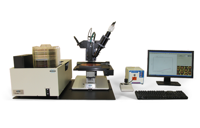
The FilmTek™ 2000 PAR benchtop spectroscopic reflectometer is an economical solution for high-throughput, fully automated mapping of patterned wafers in R&D and production environments. It is specifically designed to address a broad range of wafer-based technology applications in silicon semiconductor, LED/OLED, and data storage.
Expanding upon FilmTek 2000's proprietary DUV-NIR spectroscopic reflectometry technology, FilmTek 2000 PAR features integrated automated wafer handling, pattern recognition, and patented parabolic mirror-based micro-spot measurement capabilities (50 µm standard, down to 13 µm). This system delivers best-in-class measurement of patterned wafers that is more efficient, intuitive, and sensitive to local non-uniformity than comparable reflectometers, even on challenging samples.
The FilmTek 2000 PAR's fully integrated, advanced material modeling software supports both built-in standard and user-defined wafer map patterns, providing rapid generation of 2D and 3D data maps of any measured parameter. Optional Cognex pattern recognition, cassette-to-cassette wafer handling, and SECS/GEM compatibility can be added to further optimize the system's measurement capabilities and performance to your specific application.
Measurement Capabilities
Enables simultaneous determination of:
- Multiple layer thicknesses
- Indices of refraction [ n(λ) ]
- Extinction (absorption) coefficients [ k(λ) ]
- Energy band gap [ Eg ]
- Composition (e.g., %Ge in SiGex, % Ga in GaxIn1-xAs, %Al in AlxGa1-xAs, etc.)
- Surface roughness
- Constituent, void fraction
- Crystallinity/Amorphization (e.g., of Poly-Si, GeSbTe films)
- Film gradient
System Components
Standard:
- DUV-NIR fiber-optic spectrophotometer
- Spectroscopic reflection measurement
- Patented parabolic mirror technology
- Automated stage with autofocus
- Automated wafer handling
- Camera for imaging measurement location
- Pattern recognition
- 50 micron spot size (standard)
- Advanced material modeling software
- Bruker's generalized material model with advanced global optimization algorithms
Optional:
- Small spot size (13 µm)
- Pattern recognition (Cognex)
- Cassette to cassette wafer handling
- SECS/GEM compatibility
Typical Application Areas
Virtually all translucent films ranging in thickness from less than 100 Å to approximately 150 µm can be measured with high precision. Typical application areas include:
- Semiconductor and dielectrics
- Data storage
- LED/OLED
With flexible hardware and software that can be easily modified to satisfy unique customer requirements in R&D and production environments.
Technical Specifications
| Film Thickness Range | 3 nm to 150 µm |
|---|---|
| Film Thickness Accuracy | ±1.5 Å for NIST traceable standard oxide 1000 Å to 1 µm |
| Spectral Range | 190 nm - 1700 nm (240 nm - 1000 nm is standard) |
| Measurement Spot Size | 13 µm - 300 µm (50 µm is standard) |
| Wafer Size | 50 mm - 300 mm (150 mm standard) |
| Spectral Resolution | 0.3 - 2 nm |
| Light Source | Regulated deuterium-halogen lamp (2,000 hrs lifetime) |
| Detector Type | 2048 pixel Sony linear CCD array / 512 pixel cooled Hamamatsu InGaAs CCD array (NIR) |
| Computer | Multi-core processor with Windows™ 10 Operating System |
| Measurement Time | <1 sec per site (e.g., oxide film) |
| Data Acquisition Time | 0.2 sec |
Performance Specifications
| Film(s) | Thickness | Measured Parameters | Precision (1σ) |
|---|---|---|---|
| Oxide / Si | 200 - 500 Å | t | 0.5 Å |
| 500 - 10,000 Å | t | 0.25 Å | |
| 1000 Å | t , n | 0.25 Å / 0.001 | |
| Nitride / Si | 200 - 10,000 Å | t | 0.25 Å |
| Photoresist / Si | 200 - 10,000 Å | t | 0.5 Å |
| a-Si / Oxide / Si | 200 - 10,000 Å | t | 0.5 Å |