
SEM EDS and TEM EDS for Semiconductor Analysis
Energy Dispersive X-Ray Spectroscopy (EDS/EDX) of Semiconductors
Energy Dispersive X-Ray Spectroscopy (EDS or EDX) is a powerful analytical technique for semiconductor analysis. The semiconductor industry requires precise and comprehensive characterization of materials. EDS meets these requirements by offering fast, reliable and non-destructive elemental analysis of semiconductor materials with exceptional sensitivity and spatial resolution.
Semiconductors play a pivotal role in electronic devices, ranging from microprocessors and memory chips to sensors and integrated circuits. Chemical mapping of semiconductor devices at high spatial resolution is required to optimize their performance, ensure quality control, and to advance research and development efforts.
EDS provides a non-destructive and efficient method to analyze the elemental distribution of semiconductor samples, enabling researchers and engineers to make informed decisions about material design, manufacturing processes, and overall device functionality.
SEM EDS for Semiconductor Analysis
EDS/EDX is an indispensable tool for semiconductor analysis, allowing researchers to precisely determine the elemental composition of materials at the microscale and beyond.
SEM EDS provides crucial insights into semiconductor device structures, identifying and mapping elements to optimize device performance. This technique is particularly valuable for quality control, failure analysis, and research and development in the ever-advancing field of semiconductor technology.
Bruker's latest generation of EDS detectors, XFlash® 7, allows for unmatched analysis speeds without compromising spectral quality. Our novel detectors XFlash® 7100oval and XFlash® FlatQUAD maximize the solid angle for maximum collection efficiency and highest count rate at very low probe currents.
The ultra-high spatial resolution capable EDS detector XFlash® 7100oval has an oval shaped chip with windowless design and an active area of 100mm2 . The detector is compatible with entry-level to high-end microscopes, with or without magnetic immersion lenses, up to 30 kV for qualitative and quantitative analysis. This enables ultra-high spatial resolution chemical mapping of semiconductor features, giving analysts the opportunity to acquire TEM-like EDS mapping with SEM.
Find out more about the application of SEM EDS in the semiconductor industry with our applications and webinars below.
TEM EDS and STEM EDS for Semiconductor Analysis
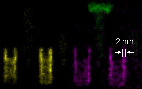
EDS/EDX with a TEM is a vital tool for semiconductor analysis, offering high-resolution elemental analysis at the nanoscale. EDS TEM enables researchers to investigate the elemental composition of semiconductor materials with exceptional spatial precision, providing crucial information for the development and optimization of nanoscale devices.
The capability of EDS TEM to map elemental distributions in thin films and nanostructures makes it an essential technique for advancing semiconductor research and ensuring the quality of cutting-edge electronic components.
Find out more about the application of TEM EDS in the semiconductor industry by viewing the applications and webinars below.
QUANTAX Systems for EDS Analysis
As shown in these application examples, Bruker's QUANTAX EDS for SEM and QUANTAX EDS for TEM systems are well suited for use in the semiconductor industry.
In addition to our industry-leading EDS technology, such as our XFlash® 7 detectors, Bruker provides application support and training.


