
Nanoscale Surface Characterization of Polymeric Materials and Products
Explore Tools and Techniques for Nanoscale Polymer Property Measurement
Attendees of this virtual Surface Lab session can expect to explore a range of characterization techniques as they are used by leading researchers in the field of polymer research.
With welcome address, introduction, live audience Q&A, and closing remarks by Dr. Peter De Wolf, Worldwide Application Director, Bruker
Introduction
- [00:01:39] Event agenda – overview of presentation topics and speakers
- [00:03:18] Introduction to the topic of nanoscale polymeric chanracterization
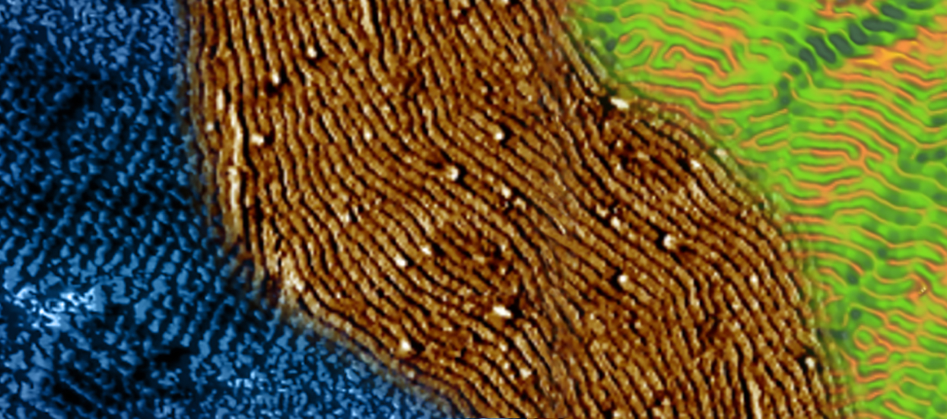
- [00:03:50] Overview of structural properties accessible via BioAFM, nanoIR, and/or nanoindentation methods
- [00:07:18] Overview of select nanomechanical, nanoelectrical, and nanothermal properties
Webinar Summary
Bruker is dedicated to providing a complete range of high-performance metrology techniques for the nanometer-scale surface characterization of polymeric materials and products. Featuring a panel of Bruker application experts, this webinar includes presentations and live technical demonstrations highlighting the features, capabilities, and practical use of Bruker's tools and techniques for nanoscale polymer property measurement. During this webinar, you can expect to:
- Gain understanding about the applications, advantages, and considerations of different property characterization methods
- View event-exclusive demonstrations of various tools and techniques for characterizing the nanoscale properties of polymeric samples
- Hear Bruker experts answer audience questions submitted by polymer researchers
Presentations topics include:
- High-resolution AFM-based measurement of nano-scale mechanical, electrical, and temperature-dependent properties
- High-performance chemical characterization via photothermal AFM-IR spectroscopy
- Nanomechanical characterization of viscoelastic properties by nanoindentation
Find out more about solutions for the characterization of polymeric materials that Bruker offers:
Webinar Overview
| Presentation Lenght | Presentation Title | Presenter | Abstract |
| 55 min | Nanoscale Topography and Advanced Physical Property Characterization Using AFM | When studying polymeric materials, AFM has many resolution and versatility benefits over alternative techniques.
The presenters cover several different AFM methods for measuring the properties of polymers, from high-resolution elastic & viscoelastic mechanical property mapping to nano-electrical and temperature-dependent measurements. | |
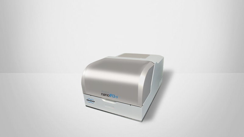
| 25 min | Nanoscale Spectroscopy and Imaging Using NanoIR – Photothermal AFM-IR Talk and live demo | Combining IR spectroscopy with the high-resolution imaging capabilities of AFM enables the chemical characterization of polymeric materials. The presenters provide insights into new and existing photothermal AFM-IR techniques and demonstrate how to achieve high-performance results. | |
| 27 min | Investigating the Influence of Environmental Conditions with Nano-Indentation | Nano-mechanical characterization can also be achieved using nano-indentation methods. The presenters in this segment:
|
Featured Products and Technology


Speakers

Peter De Wolf, Ph.D., Director of Technology & Application Development
Peter De Wolf is director for AFM technology & application development at Bruker Nano Surfaces, covering all applications related to Scanning Probe Microscopy (SPM). He obtained his PhD from IMEC, Belgium on the development of new SPM methods for 2D carrier profiling in semiconductors and has more than 25 years of experience on SPM. He is the author and co-author of over 30 publications related to electrical characterization using SPM. He also owns several SPM patents, and developed several new SPM modes for electrical characterization.

Heiko Haschke, Ph.D., Application Scientist, Bruker
Heiko Haschke received his Ph.D. in physics from the University of Bristol, UK, where he focused on the application and development of high-speed imaging and force spectroscopy for studying single biomolecular interactions. In 2001, he joined JPK Instrument AG as a developer of nanoanalytical instrumentation, in particular, AFMs and optical tweezers for biological applications. In 2004, he set up and became head of the Applications group, a team of applications scientist experts, providing worldwide customer and technical support. Since 2020, he is overseeing the worldwide applications development of the NanoRacer® high-speed AFM, from the BioAFM unit of Bruker Nano, based in Berlin, Germany.

Mickael Febvre, Ph.D.
Application Manager, Bruker EMEA

Miriam Unger, Ph.D.
Applications Manager EMEA, NanoIR, Bruker Nano GmbH

Hartmut Stadler, Ph.D., Application Scientist, Bruker

Thomas Henze, Ph.D., BioAFM Application Scientist, Bruker

Ude Hangen, Ph.D.
Applications Manager, Bruker EMEA

Jaroslav Lukeš, Ph.D., Sales Applications Scientist, Bruker

