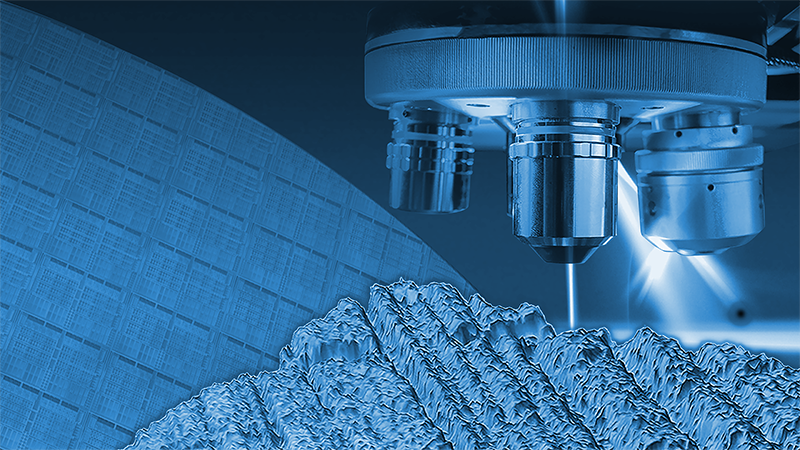

Introducing the New NPFLEX-1000 3D Optical Profiler: Automated Surface Characterization of Large Samples and Complex Geometries
See how our latest technology solves unique challenges in QA/QC for large industrial parts and complex geometries.
In this event, Bruker experts discuss and demonstrate the leading-edge technology and capabilities that make the NPFLEX-1000 uniquely well-suited for use in diverse, dynamic production environments.
Viewers can expect to:
- Find out what the NPFLEX-1000 can do for operators in industrial applications spaces such as precision machining, additive manufacturing, aerospace, orthopedics/ophthalmics, and more;
- Understand how the NPFLEX-1000 enables both non-contact, 3D characterization of surfaces and quantification of wear and corrosion;
- See how the NPFLEX-1000 works in a live exhibition of the system being used to measure large, complex industrial parts and samples; and
- Learn how to use it as our experts explain and demonstrate how to measure surfaces inside of a cylinder.
Webinar Summary
The automated, floor-standing NPFLEX-1000 brings gage-capable measurement and analysis capabilities to manufacturing industries for fast, flexible evaluation of nano- to macro-features on large industrial parts. Applications range from measuring surface roughness, local curvature, and waviness to the identification of defects.
This webinar consists of two presentations and two live demonstrations, as well as a live Q&A session. A team of four Bruker experts discuss situations in which the system's large-sample capabilities, flexible evaluation options, and automated measurement and analysis features could make NPFLEX-1000 an ideal solution. Viewers are also introduced to key features, such as its:
- Large, open-gantry bridge;
- Swivel head with a 300 mm distance between stage and objectives;
- Long working distance objectives; and
- Fold mirror option.
Find out more about the technology featured in this webinar or our other solutions for Optical Profilometry:
| Presentation Lenght | Presentation Title | Speaker |
|---|---|---|
| 16 min | NPFLEX-1000 3D Optical Profilometer for Large Samples and Complex Geometries | Dr. Mickael Febvre, Applications Manager Europe, Bruker France |
| 1 min | Live Demo: Introducing Key Components | Dr. Ravi Chintala, Applications Scientist, Bruker USA |
| 10 min | Challenging Characterization Applications: Large Samples & Complex Geometries | Dr. Mickael Febvre |
| 9 min | Live Demo: Measuring Inside Cylinders with a Fold Mirror | Dr. Udo Volz, Applications Engineer, Bruker Germany |
| 7 min | Q&A | - |
Featured Products and Technology
Speaker(s)
Sandra Bergmann,
Product Marketing Engineer, Bruker Austria
Mickael Febvre, Ph.D.
Application Manager, Bruker EMEA
Udo Volz, Ph.D.
Applications Engineer, Bruker EMEA
Ravi Chintala, Ph.D.
Application Scientist, Bruker Nano SurfacesRavi Chintala is currently working as Application Scientist at Bruker Nano Surfaces. Ravi Chintala, has more than 10 years of research experience on scanning probe microscopy, focusing specifically on various electrical SPM techniques. Before starting his career as an Application Scientist at PrimeNano,Inc., Dr. Chintala was a postdoctoral fellow at Lawrence Berkeley National Laboratory investigating nanoscale charge carrier dynamics of solar cells using KPFM. Dr. Chintala has obtained his PhD from IMEC, (Belgium) and MS from Michigan Technological University (Houghton, MI).


