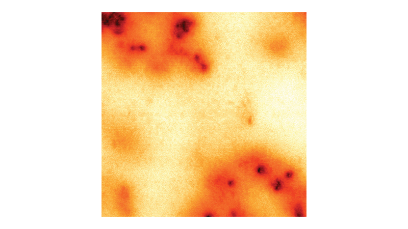
Characterization of Thin Dielectric Films with Atomic Force Microscopy
Learn how AFM can be applied to measure and quantify the properties of dielectric film.
Topography and Conductivity Based Measurements
PRESENTATION HIGHLIGHTS:
- [00:00:00] Introduction to the AFM technique
- [00:01:09] Typical applications in dielectrics
- [00:03:54] Electrical properties measurable by AFM
- [00:04:53] Conductive AFM (C-AFM)
- [00:06:29] Tunneling-AFM (TUNA)
- [00:12:34] DataCube TUNA
Live Demo - Tunneling AFM on Dimension Icon AFM
PRESENTATION HIGHLIGHTS:
- [00:00:11] Instrument setup and sample
- [00:01:30] Software configuration
- [00:02:52] Data acquisition
- [00:04:07] Generating an I-V curve
- [00:05:54] Data images and interpretation
Charge and Capacitance Based Measurements
PRESENTATION HIGHLIGHTS:
- [00:00:14] Scanning Microwave Impedance Microscopy (sMIM)
- [00:06:47] Kelvin Probe Force Microscopy (KPFM)
- [00:09:15] Extract ε from capacitance measurements between the tip and sample
- [00:10:40] Electrostatic Force Microscopy (EFM)
Live Demo - Scanning Microwave Impedance Microscopy on Dimension Icon AFM
PRESENTATION HIGHLIGHTS:
- [00:00:00] Experimental setup
- [00:02:16] Data acquisition
- [00:05:14] Generating capacitance-distance curves
Advanced AFM Characterization
PRESENTATION HIGHLIGHTS:
- [00:00:11] Measurements on cross-sectioned devices
- [00:00:59] PiezoResponse Force Microscopy (PFM)
- [00:03:17] Chemical property characterization by AFM-IR
- [00:05:58] Other techniques for characterizing dielectric materials
Q&A
PRESENTATION HIGHLIGHTS:
- [00:00:00] What is the difference between C-AFM and TUNA and what is the maximum TUNA current?
- [00:01:06] Can one get similar conductive AFM graphs on wide band gap semiconductors?
- [00:01:48] How many I-V curves are recorded per pixel and is the I-V curve generated an average of multiple recordings?
- [00:02:57] Are these kinds of conductivity measurements with TUNA also possible on materials that are less insulating or more bulky? (e.g., low band gap semiconductors, like silicon substrates or germanium)
- [00:04:11] Is it possible to use KPFM to estimate the size of the depletion region in a PNP semiconductor device structure via the static charge distribution?
- [00:05:51] What are the challenges for electrical measurements on softer samples and biological samples (e.g., neuronal cells that are also known to conduct electrical signals)?
- [00:07:58] What materials can be detected by AFM-IR (on the Dimension IconIR system)?


