
AFM for Critical Dimension: Metrology of Trenches, Lines and Gratings
Characterizing critical dimensions of various component structures is an essential step to provide quality control feedback on fabrication processes
In this webinar, Bruker AFM experts discuss and demonstrate the applications of AFM in the characterization of trenches, lines, and gratings, including a real-time demonstration of how to measure a patterned sample with our Dimension AFM and AutoMET software option.
Non-Destructive Critical Dimension Measurement with Nanometer Accuracy
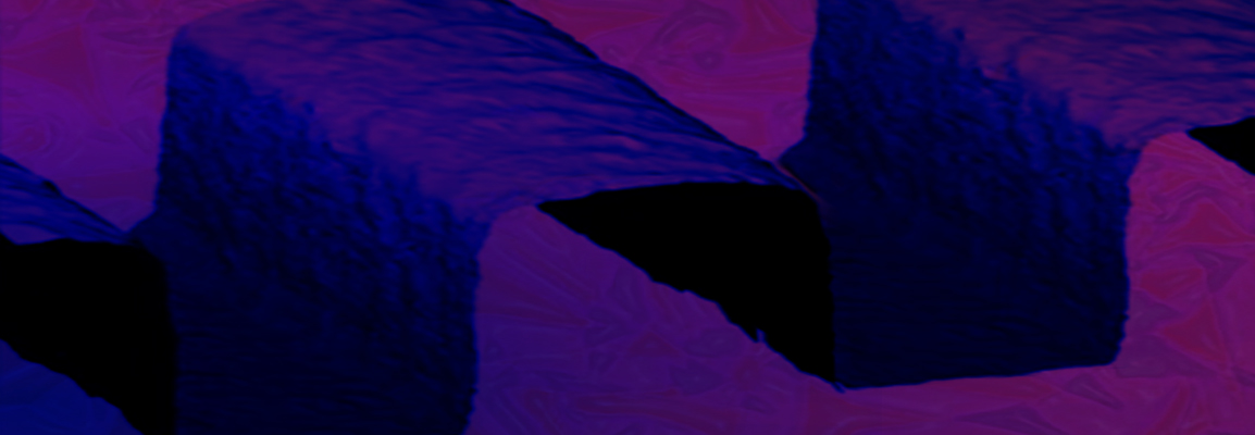
Electronic devices are getting smaller and more efficient, and thus require higher quality in the inspection of semiconductor microfabrication processes. Current technology features component structures (e.g., trenches, lines, and gratings) that measure down to a couple of hundred nanometers. This scale excludes the use of optical microscopes due to the light diffraction limit. However, atomic force microscopy (AFM) can provide nanometer accuracy in x, y, and z directions without damaging components and, therefore, is a very useful tool for characterizing these structures.
In this workshop, Bruker applications experts Senli Guo, Ph.D. (Sales Applications Engineer, Bruker) and John Thornton (Engineer Sr. Applications, Bruker) discuss and demonstrate:
- The applications of AFM for critical dimension measurement
- Bruker's Dimension AFM, a large‑platform system that utilizes proprietary PeakForce Tapping mode for superior critical dimension measurement performance;
- AutoMET, our AFM software option for automatically measuring samples with the help of pattern recognition;
- The offline batch data process specifically for trenches, lines, gratings, and similar structures.
The workshop concludes with a real-time demonstration showing how to measure a patterned sample and an expert-led Q&A session with the live workshop audience.
Find out more about the technology featured in this webinar or our other solutions for surface measurement:
Featured Products and Technology
Speakers
Senli Guo, Ph.D., Application Scientist, Bruker
Senli earned his Ph.D. in physical chemistry from Duke University (2009) and spent two years in the Center for Nanophase Materials Sciences (CNMS) at Oak Ridge National Lab as a postdoc before joining Bruker as an applications scientist in 2011. All of Senli’s research is about AFM-based methodology developments to address various nanoscience research, ranging from single-molecule interactions to lithium-ion battery electrode properties.
John Thornton,
Senior Application Scientist, BrukerJohn Thornton is a Senior Applications Engineer at Bruker Nano Surfaces with 25+ years of experience in the field of Atomic Force Microscopy (AFM). He learned AFM at North Carolina State University in the 1990s, and then joined Digital Instruments, a pioneering company in early AFM development, and continued with the company through acquisitions by Veeco Instruments, and then Bruker. John has co-authored many scientific publications and developed scanning probe microscopy training courses. Currently, John spends a significant amount of time running AFMs and educating others on techniques. He currently works from his home in Virginia, and from the Bruker AFM applications lab in Billerica, MA.

