FilmTek 3000M
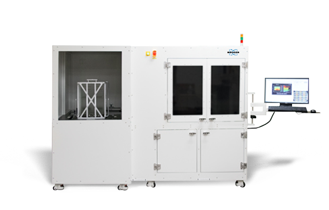
FilmTek 3000M
The FilmTek™ 3000M micro-spot reflection-transmission metrology system enables efficient and accurate measurement of patterned films deposited on transparent substrates, including wafers. Moreover, it outperforms the micro-spot measurement capabilities of conventional systems, even on non-uniform samples, and can characterize films far thicker than competing instruments can accommodate.
Conventional micro-spot film metrology systems use high-power objectives, making them prone to significant signal degradation and optical artifacts. Conversely, FilmTek 3000 uses our patented microscope-based optical design — characteristic of all our "M" series instruments — featuring a low-power objective with a nearly collimated beam. It is consequently able to achieve a measurement spot size down to 2 µm with consistently high signal fidelity during small- and micro-spot measurements. As a result, FilmTek 3000M delivers spectral reflection and transmission measurements with maximum signal coherence, providing best-in-class accuracy and reliability on samples not easily or feasibly measured with conventional instruments.
Options are available to optimize FilmTek 3000M's design for more specialized measurements, including large custom sample stages for flat panel display applications. This system can also be configured to provide fully-automated imaging-based critical dimension (CD) measurement of patterned samples, allowing for simultaneous CD and film thickness measurement.
Measurement Capabilities
Enables simultaneous determination of:
- Multiple layer thicknesses
- Indices of refraction [ n(λ) ]
- Extinction (absorption) coefficients [ k(λ) ]
- Energy band gap [ Eg ]
- Critical dimension (CD) measurement
System Components
Standard:
- Spectroscopic reflection measurement
- Spectroscopic transmission measurement
- Patented microscope-based optical design allowing sub-10µm spot with a low power objective
- 5 nm - 50 um thickness range
- 2 um spot size (5x10 um standard)
- Automated stage with autofocus
- Camera for imaging measurement location
- Pattern recognition
- Large custom stage for flat panel display applications
- Advanced material modeling software
- Bruker's generalized material model with advanced global optimization algorithms
Optional:
- Automated flat panel/wafer handling
- Flat panel total thickness variation (TTV) measurement
- SECS/GEM
Typical Application Areas
Typical application areas include:
- Wafer/CD metrology
- Flat panel display
With flexible software that can be easily modified to satisfy unique customer requirements in R&D and production environments.
Technical Specifications
| Film Thickness Range | 5 nm to 350 µm (5 nm to 150 µm is standard) |
|---|---|
| Film Thickness Accuracy | ±1.5 Å for NIST traceable standard oxide 1000 Å to 1 µm |
| Spectral Range | 380 nm - 1700 nm (380 nm - 1000 nm is standard) |
| Measurement Spot Size | 2 µm (5x10 µm standard with 10x objective) |
| Sample Size | 2 mm - 600 mm (150 mm is standard) |
| Spectral Resolution | 0.3 - 2 nm |
| Light Source | Regulated halogen lamp (2,000 hrs lifetime) |
| Detector Type | 2048 pixel Sony linear CCD array / 512 pixel cooled Hamamatsu InGaAs CCD array (NIR) |
| Computer | Multi-core processor with Windows™ 10 Operating System |
| Measurement Time | <1 sec per site (e.g., oxide film) |
Performance Specifications
| Film(s) | Thickness | Measured Parameters | Precision (1σ) |
|---|---|---|---|
| Oxide / Si | 500 - 1000 nm | t | 0.025 nm |
| 1 - 150 µm | t | 0.005% |