
Nanoelectrical Characterization Using Atomic Force Microscopy
Choose the best method for measuring the nanoelectrical properties of your sample.
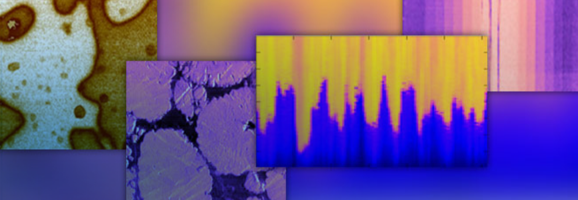
Atomic force microscopy (AFM) has unique capabilities that make it ideal for nanoscale electrical characterization of properties including conductivity, resistivity, work function, surface potential, charge/carrier density, and dielectric/piezoelectric properties.
Watch this webinar to learn about:
- Our experts' recommendations for AFM modes for characterizing different nanoelectrical properties, supported using example data showing results on a variety of materials and devices.
- The key challenges and advantages of common AFM modes used for nanoelectrical characterization.
- Practical considerations for nanoelectrical characterization, including tip/cantilever selection, influence of environment, and quantification possibilities.
- How nanoelectrical data can be correlated with AFM-based nanomechanical and nanochemical data.
Abstract
In this webinar, the presenters highlight how atomic force microscopy (AFM) is ideally suited for nanoscale characterization of electrical properties, including conductivity, resistivity, work function, surface potential, charge. carrier density, dielectric and piezo-electric properties.
The presenters will first give an overview of available AFM modes commonly applied in nanoelectrical material research and describe their advantages and challenges. They will illustrate each mode with a few examples on a variety of materials and devices including semiconductors, 2D materials, batteries, and photovoltaics. They will then address practical aspects, such as selecting the ideal AFM tip and cantilever, influence of the environment, and quantification possibilities.
The presenters will also discuss how the high-resolution imaging capability of these AFM modes can be complemented by local spectroscopy, such as I-V, C-V and domain switching spectroscopy in selected positions, as well as in complete maps through DataCube approaches. Finally, they will describe how these nanoelectrical properties can be correlated with AFM-based nanomechanical and nanochemical characterization data.
Find out more about the technology featured in this webinar or our other solutions for nanoelectrical characterization:


Speakers

Peter De Wolf, Ph.D., Director of Technology & Application Development
Peter De Wolf is director for AFM technology & application development at Bruker Nano Surfaces, covering all applications related to Scanning Probe Microscopy (SPM). He obtained his PhD from IMEC, Belgium on the development of new SPM methods for 2D carrier profiling in semiconductors and has more than 25 years of experience on SPM. He is the author and co-author of over 30 publications related to electrical characterization using SPM. He also owns several SPM patents, and developed several new SPM modes for electrical characterization.

Khaled Kaja, Ph.D., Applications Scientist
Dr. Khaled Kaja holds a PhD in Nanophysics from the University of Grenoble. He started his research journey at the Leti laboratory (French commission of atomic and alternative energies, CEA) working on the development of highly-resolved nanoelectrical AFM measurements. Following a post-doctoral training at the Swiss federal institute (ETH) Zurich under the chair of nanotechnology (Prof. Dr. Andreas Stemmer), he moved to the UK joining Bruker nano surfaces as an applications scientist. In 2017, Dr. Kaja moved to the middle east as an assistant professor of physics at different universities in the region. Later in 2020, he joined the French national metrology lab (LNE) as a research scientist working on the development of nanoelectrical metrology. Recently, Dr. Kaja joined Bruker nano surfaces and metrology in Karlsruhe (Germany) as an applications scientist. His main research interests are focused on the development of novel nanoelectrical AFM methods applied to 2D materials and low dimensional systems.