Application of Atomic Force Microscopy in the Study of Semiconductor Materials and Devices
Key Topics
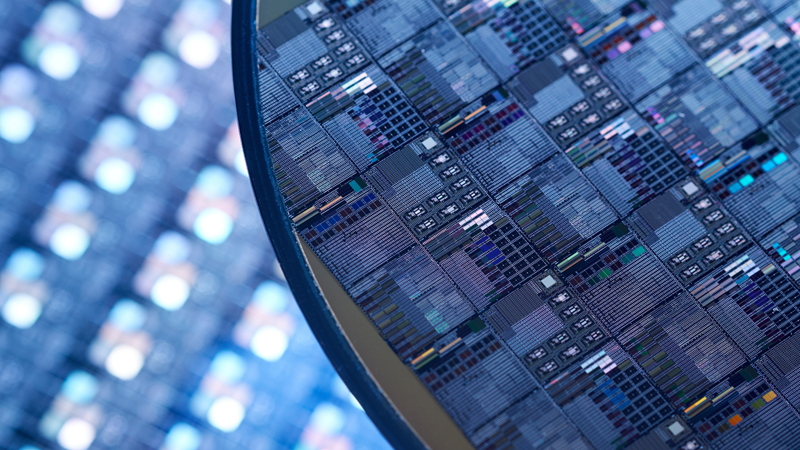
Our speakers take a closer look at the capability of industry-leading AFM technology to perform high-resolution imaging of surface topography. A few typical applications are covered, including:
- Roughness characterization of bare wafers and thin films;
- CMP characterization including roughness, dishing and erosion;
- Inspection of nanoscale defects; and
- Critical dimension metrology of lines, trenches, holes and other nanoscale structures such as CMOS imaging sensor micro lenses and LED patterned sapphire substrate dome structures.
Practical aspects such as tip selection, tip shape monitoring and tip lifetime, throughput, automation and extraction of critical analysis parameters are also discussed.
Finally, the webinar closes with an exploration of the capability to apply AFM for local chemical identification by combining it with nanoscale IR imaging and spectroscopy. Two interesting applications of this ‘AFM-IR’ approach are the chemical identification of contaminants and chemical mapping (with 10 nm spatial resolution) of specific materials.
This webinar was presented on: December 16, 2020
Speakers

Peter De Wolf, Ph.D., Director of Technology & Application Development
Peter De Wolf is director for AFM technology & application development at Bruker Nano Surfaces, covering all applications related to Scanning Probe Microscopy (SPM). He obtained his PhD from IMEC, Belgium on the development of new SPM methods for 2D carrier profiling in semiconductors and has more than 25 years of experience on SPM. He is the author and co-author of over 30 publications related to electrical characterization using SPM. He also owns several SPM patents, and developed several new SPM modes for electrical characterization.

Ingo Schmitz, Ph.D.
Technical Marketing Engineer, Bruker
Ingo Schmitz received his Ph.D. in Chemistry from the University of Technology, Vienna Austria in 1996. His Ph.D. work focused on the development of SPM-based in-situ characterization of corrosion processes of glass and metal surfaces. Since 1997, Ingo Schmitz works at Bruker (formerly Digital Instruments & Veeco Instruments) in both Santa Barbara, USA. At Bruker, he held positions as an R&D engineer and application development scientist and contributed in the development of SPM methods including automated surface characterization of polysilicon. Currently, he is working in the technical marketing of automated AFM systems.