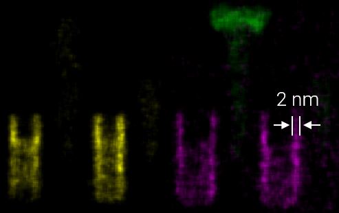

Ultra-High Spatial Resolution EDS Mapping of Semiconducting Materials with FEG-SEM
Ultra-High Resolution Elemental Mapping of Semiconductors
To fully accommodate the required computing speeds of emerging technologies, semiconductor fabricators are aiming to achieve higher processing speeds by improving the 3D device (FinFET and GAAFET) structure and the use of new materials.
The characterization of semiconductor devices is vital but challenging since their finest features are smaller than 1 nm. Transmission electron microscopes equipped with elemental analyzers, such as EDS (and EELS) detectors, are often used for such work.
This webinar presents the strengths of SEM EDS for the chemical mapping of complex structures in bulk and of electron transparent specimens at a high spatial resolution.
Failure analysis of modern sub 20 nm technology node CPUs often requires samples to be deprocessed to the layer of interest, or the preparation of thinned sample sections, i.e., lamellae. The Xe Plasma FIB-SEM system TESCAN SOLARIS X provides a dedicated method for the deprocessing of semiconductor chips called gas-assisted delayering, whereas the Ga FIB-SEM system TESCAN SOLARIS prepares site-specific lamellae with a thickness comparable to the technology node size. In this webinar approaches using both systems will be explored.
Furthermore, we show how ultra-high spatial resolution chemical distribution maps can be acquired using SEM EDS. The oval-shaped 100mm2 windowless X-ray detector XFlash® 7100oval can be used to acquire chemical maps with a nanometer resolution in a SEM. The system's oval detector head geometry and slim-line design enable EDS analysis at a large solid angle of up to 0.4 sr with a high collection efficiency.
The side entry annular XFlash® FlatQUAD EDS detector with an even larger solid angle of up to 1.1 sr and unique sample-detector geometry provides the highest sensitivity for low kV low probe current EDS measurements in SEM available on the market.
Who Should Watch this Webinar?
- Failure analysis engineers and FIB/SEM microscopists working with semiconductor labs and fabrications interested in advanced analytical techniques.
- SEM and TEM users interested in the characterization of nanostructured materials.
- Everyone working within materials science, life science and academia interested in advanced elemental analysis.
Speakers
Maksym Klymov
Senior Application Specialist – Semiconductors, Tescan Orsay Holding, Brno, Czech Republic
Dr. Purvesh Soni
Sr. Applications Scientist EDS, Bruker Electron Microscope Analyzers
Watch this Webinar On-Demand
Please enter your details below to gain on-demand access to this webinar.


