
Surface Characterization of Semiconductors: An Overview, from Topography to Advanced Physical Properties
Discover the most impactful innovations in semiconductor research.
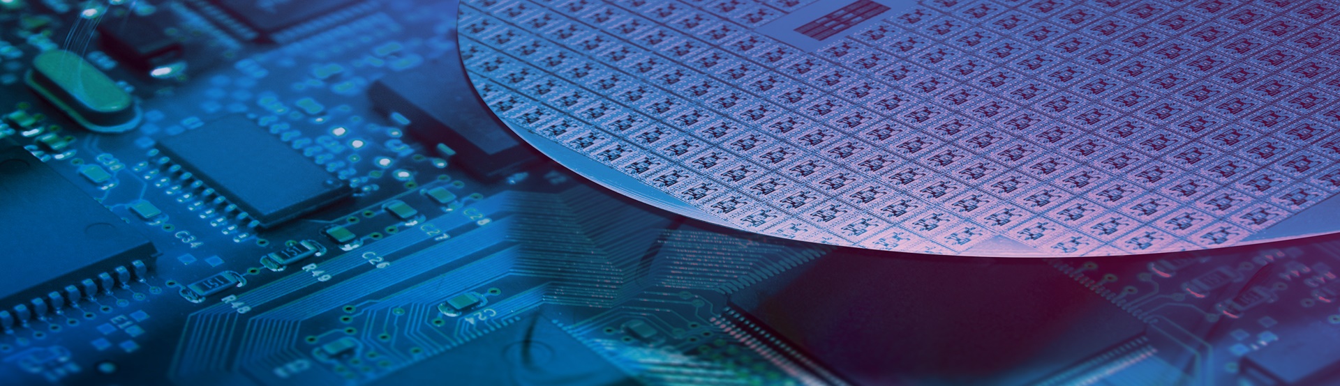
This presentation focuses on Bruker’s solutions for nanometer-scale surface characterization of semiconductor materials and devices and the common questions and challenges facing scientists in this field. See real-time demonstrations of Bruker technology and the latest and most effective techniques available to semiconductor materials researchers.
Webinar Summary
Discover The Latest in High-Performance Surface Metrology
This workshop highlights how Bruker’s high-performance metrology techniques can provide new impulses for your research and assist in the nanometer-scale surface characterization of semiconductor materials and devices.
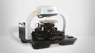
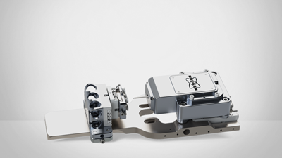
Our automated metrology solutions enable the streamlining of nanomechanical property sampling, from nanoscale-to-microscale indentation to surface roughness measurement, chemical mechanical planarization (CMP), and etch-depth measurements on the most current technology nodes and wafers.
We demonstrate the capabilities of high-resolution, in-situ scanning probe microscopy (SPM) imaging, high-speed mechanical property mapping, and Optical (WLI) Profiling and Stylus Profiling to provide an in-depth explorationof material behavior at the nanoscale, ideal for R&D and the monitoring and improvement of manufacturing processes.
This webinar was presented on April 21, 2021.
Find out more about the technology featured in this webinar or our other solutions for surface characterization of semiconductor materials:
Featured Products and Technology


Speakers

Peter De Wolf, Ph.D., Director of Technology & Application Development
Peter De Wolf is director for AFM technology & application development at Bruker Nano Surfaces, covering all applications related to Scanning Probe Microscopy (SPM). He obtained his PhD from IMEC, Belgium on the development of new SPM methods for 2D carrier profiling in semiconductors and has more than 25 years of experience on SPM. He is the author and co-author of over 30 publications related to electrical characterization using SPM. He also owns several SPM patents, and developed several new SPM modes for electrical characterization.

Samuel Lesko, Ph.D.
Dir. of Technology and Apps Development for Tribology, Stylus & Optical Profilers, Bruker
Samuel Lesko has over 20 years of optical and stylus profiler applications experience, particularly in using white-light interferometry in a wide variety of fields, from MEMS and semiconductor to automotive and aerospace. He is a member of SME and part of ISO/TC 213/WG committee (areal roughness) and obtained his physics Ph.D. and material science engineering degree at the University of Burgundy in France.

Mickael Febvre, Ph.D.
Application Manager, Bruker EMEA

Udo Volz, Ph.D.
Applications Engineer, Bruker EMEA

Ude Hangen, Ph.D.
Applications Manager, Bruker EMEA
Vishal Panchal, Ph.D.
Sales Applications Scientist, Bruker EMEA

Hartmut Stadler, Ph.D.
Applications Engineer, Bruker Nano GmbHHartmut Stadler works as an application scientist for Bruker Nano Surfaces and is now mainly focussed on the chemical side of AFM, including electrochemical operation and nanoscale IR techniques. His background is Physical Chemistry, with a PhD thesis in the field of biofilm characterization using macroscopic and nanoscopic methods. Since more than 25 years he operates AFMs and since more than 20 years he supports Bruker’s European AFM customers and distribution channel partners in AFM-application related questions.

