
In Situ SEM Nanomechanics with Bruker’s PicoIndenter
See what experts are doing with in-situ SEM nanomechanical testing
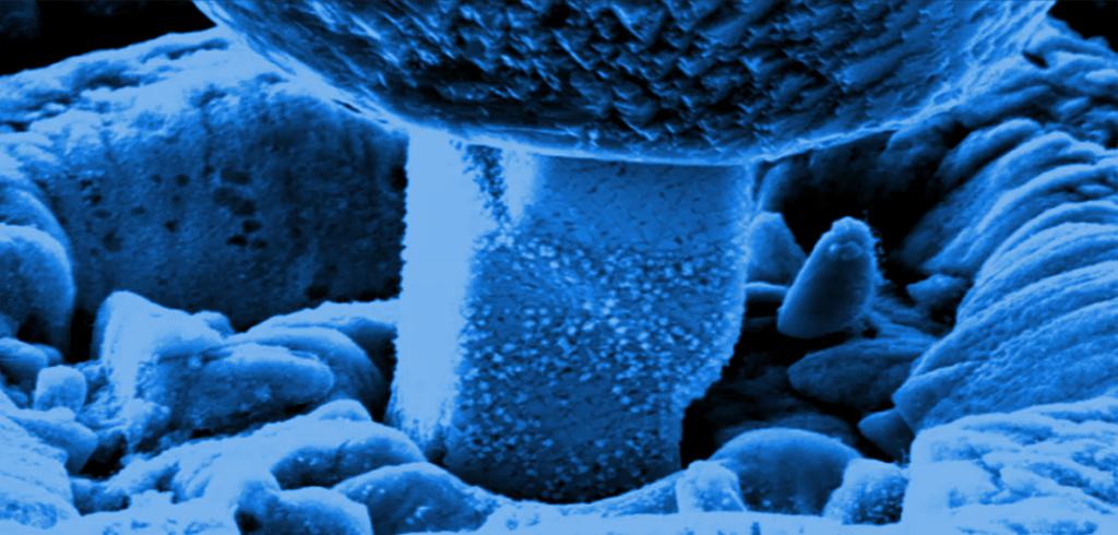
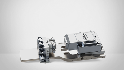
Bruker’s in-situ SEM PicoIndenters enable unique insight into material deformation behavior. The latest addition to the PicoIndenter product portfolio is PI 89, which introduces ease-of-use upgrades and a streamlined design.
This webinar contains four main segments:
- Material Properties at Cryogenic Temperatures, a guest presentation by Dr. Peter Hosemann (UC Berkeley)
- Introduction to the PI 89 SEM PicoIndenter, presented by Dr. Sanjit Bhowmick (Bruker)
- Demonstration of PI 89, presented by Dr. Eric Hintsala (Bruker)
- Mechanical Stability of Advanced Nano-Interconnects, a guest presentation by Dr. Kris Vanstreels (imec)
Webinar Summary
In-situ nanomechanical testing inside a scanning electron microscope (SEM) provides unique insight into material dynamics at small length scales. This webinar is a wide-ranging overview of SEM PicoIndenter topics, from introducing the newest Bruker tool to cryogenic testing being conducted in academia and semiconductor device testing at an industry lab.
After a brief introduction to the webinar, Dr. Peter Hosemann presents on his work investigating material properties at cryogenic temperatures. His interests lie in addressing, fundamentally, why and how materials change their properties at different temperatures. Dr. Hosemann discusses the relevant literature on nanomechanical testing at cryogenic temperatures and shows results correlating electron backscatter diffraction and mechanical testing data for solder joints and ultrafine-grained (UFG) copper.
Bruker nanomechanics expert Dr. Sanjit Bhowmick then discusses the design and capabilities of Bruker’s Hysitron PI 89 SEM PicoIndenter, and Dr. Eric Hintsala follows with a detailed demonstration of the instrument. This demonstration includes pictures and videos of hardware elements and plots and descriptions of experimental data from high-temperature testing.
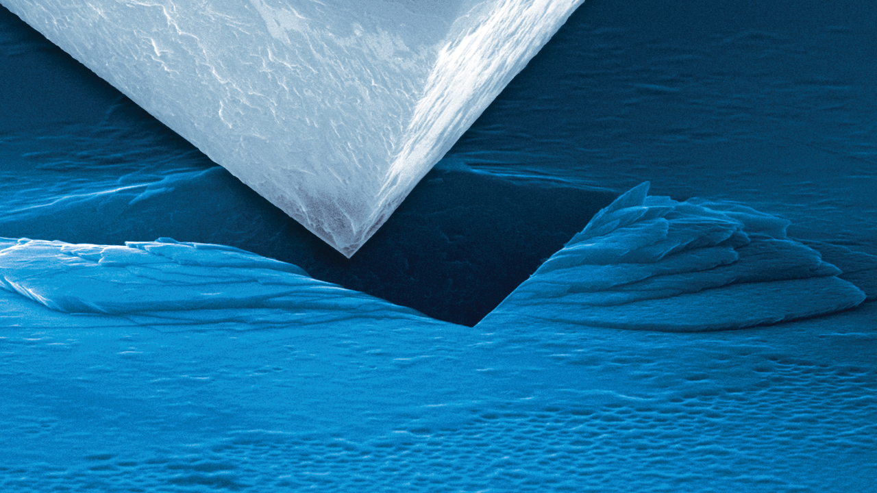
Dr. Kris Vanstreels closes with an in-depth discussion of back end of line (BEOL) strength testing and benchmarking chip-package interaction (CPI) integrity of nano-interconnects. A PI 88 SEM PicoIndenter was used in several modes for the BEOL strength testing work: indentation, compression, and bending. For the CPI investigation, a wedge indenter was used to induce and analyze thin film delamination.
Find out more about the technology featured in this webinar or our other solutions for In-Situ SEM Nanomechanics:
Featured Products and Technology
Speakers
Dr. Kris Vanstreels
Researcher, IMECKris Vanstreels received the Master of Science degree in Physics from KU Leuven in 2001 and the PhD degree in Physics from UHasselt in 2007. From 2001 to 2007, he was working as a researcher at the institute of materials research of UHasselt, where he was involved in the physical characterization of different materials systems and the development of high resolution in-situ measurement techniques. From November 2007 on he joined the Reliability and Modeling group of IMEC in Belgium as a researcher. His main research activities are focused on mechanical characterization and reliability of back-end-of-line stacks and 3D stacked-ICs.
Dr. Peter Hosemann
Professor, University of California, BerkeleyDepartment of Nuclear Engineering at the University of California, Berkeley, USA
Dr. Eric Hintsala
Applications Scientist
Dr. Eric Hintsala is a Materials Scientist, with a B.S. from Michigan Technological University and Ph.D. from the University of Minnesota. Dr. Hintsala's background is in mechanical properties of materials, nanomechanical testing techniques, and electron microscopy. Dr. Hintsala is part of R&D at Bruker NI, where he develops advanced instrumentation and testing techniques. Topics of particular interest include in situ testing, elevated temperature “in operando” testing and high speed nanoindentation mapping.
Sanjit Bhowmick, Ph.D.
Senior Staff Scientist, Bruker
Dr. Sanjit Bhowmick is a Senior Staff Scientist at Bruker. His research interest includes understanding microstructure and mechanical property correlation of advance nanostructured materials using in-situ SEM and TEM nanomechanical techniques. He has published more than 80 papers in peer-reviewed journals.


