
What is WDS? Introducing Wavelength Dispersive Spectroscopy
WDS (Wavelength Dispersive X-ray Spectroscopy) is a complementary technique to EDS (Energy dispersive X-ray Spectroscopy) analysis on a SEM. Both techniques analyze the characteristic X-rays emitted from the sample excited by the electron beam.
WDS is based on X-ray diffraction to select wavelengths of interest. With EDS, a wide range of all X-ray energy lines are collected simultaneously whereas WDS can only measure a single X-ray or one element at a time. WDS technology has the advantage that it offers a much higher spectral resolution and a much better signal-to-noise ratio.
WDS can be considerably more accurate for the analysis of samples with X-ray line overlaps and trace elements than EDS. Furthermore, when a WD spectrometer is based on a parallel beam optic (like the Bruker XSense) it is also very sensitive to the low X-ray energies. Like EDS, WDS can be used for spot analysis as well as for element distribution maps and concentration profiles. WDS relies on standards for quantification.
To find out more about how WDS works, the different kinds of detectors used and more keep on reading!
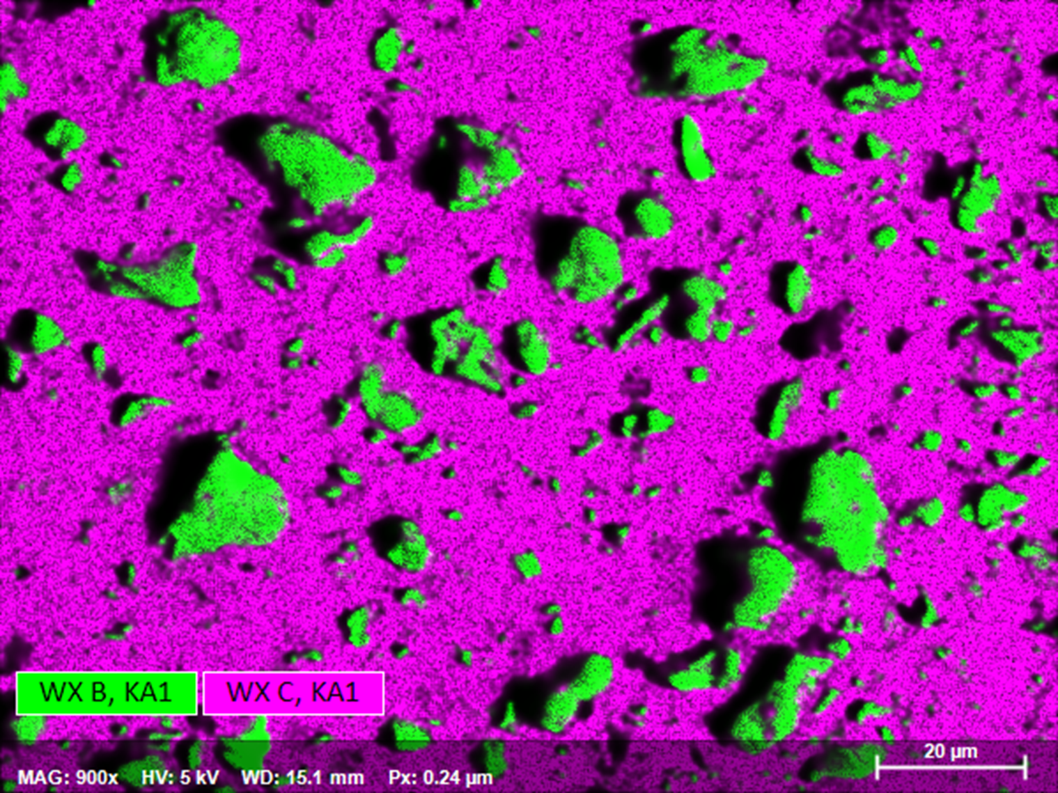
Figure 1. Elemental map acquired with WDS - the light element sensitivity of WDS allows boron to be mapped quickly, even in low concentration and where overlaps are present.
How Does WDS Work?
The characteristic X-rays emitted by the sample are diffracted by a diffractor and counted by a proportional counter used as the X-ray detector.
The wavelength analyzed by the X-ray detector is determined by the angle of incidence, theta (Θ), which is the angle of the incoming X-ray beam on the diffractor. In order to count X-rays of a specific wavelength Θ needs to be adjusted. Since the sample in the SEM remains in a fixed position Θ is adjusted by rotating the diffractor relative to the sample. In this way a range of X-ray energies can be analyzed sequentially using WDS. The elemental composition of the sample is calculated by measuring the X-ray intensity at different wavelengths.
To cover the entire energy range, several diffractors with varying d-values (crystal lattive constant of the diffractor) are required. The elemental composition of a sample is calculated from the net counts of pre-selected element lines based on peak and background measurements and a comparison with the respective net counts of standards. For purely qualitative information, sections of the wavelength spectra are scanned by continuously changing Θ during measurement.
Figure 2. Diagram showing diffraction by Bragg's law. Only X-rays of one specific wavelength will be reflected at a time. By changing the angle of incidence (θ) different wavelengths (λ) can be selected for analysis.
What are the Different Types of WDS Detectors?
Wavelength Dispersive (WD) spectrometers are available in two different designs:
- Classical WD spectrometers based on the Rowland circle geometry are commonly used on electron microprobe analyzers but are also available for SEMs.
- Parallel beam optic WD spectrometers.
Rowland Circle WD Spectrometers
In a Rowland circle based WD spectrometer all three main components, the sample, the diffractor, and the detector are situated on a circle with constant diameter.
The wavelength of the X-rays diffracted into the detector are selected by varying the angle and the position of the analyzing diffractor with respect to the sample. In order to maintain the correct geometry and to satisfy Bragg’s law the distance from the sample to the diffractor and the distance from the diffractor to the detector needs to be the same which results in different solid angles for different X-ray energies.
Figure 3. Schematic of a Rowland Circle WD Spectrometer.
Parallel Beam Optic WD Spectrometers
In a parallel beam optic WD spectrometer, an X-ray optic is placed near the sample where it transforms X-rays diverging from the sample into a parallel beam hitting the analyzer diffractor. Since the parallel beam optic stays close to the sample, the solid angle is large and allows it to capture a maximum of the emitted X-rays. From the analyzer diffractor, a monochromatic X-ray beam is reflected towards the flow proportional counter where the intensity of the selected wavelength is determined.
Since a complex Rowland circle geometry is not needed, the mechanical complexity and fragility of the spectrometer design is dramatically reduced. Due to the more compact design of a parallel beam optic WD spectromer it is easily integrated into SEMs and can be adapted either on a WDS port or even on a standard EDS port.
Figure 4. Schematic of a parallel beam optic WD spectrometer.
The Solid Angle
The solid angle describes the amount of signal collected by the detector and is calculated as the ratio of the detector surface (diffractor surface for WDS) over its distance to the source in squared function (Ω = A / D²).
The solid angle dramatically decreases with increased distance between the sample and the detector. Because of this relationship a parallel beam optic WDS that characteristically captures the X-rays very close to their source of origin has a much higher solid angle than a classical Rowland circle-type WDS. This results in significantly higher count rates for very low X-ray energies, such as those of the light elements (Z = 4-9).
Light element detection is difficult for other X-ray spectrometry methods such as EDS and classical Rowland circle-type WD spectrometer, due to the low fluorescence yield, high degrees of absorption and low quantum efficiencies of those detectors.
Elemental Mapping using WDS
WDS mapping works differently compared to EDS. Since rastering the electron beam over larger areas (low SEM magnifications) will violate Braggs Law, WDS mapping is performed by moving the SEM stage while keeping the electron beam in spot mode or at very high SEM magnification. Since this approach results in long acquisition times WD mapping with Bruker XSense works by the combination of e-beam rastering over a small field and SEM stage movement. This approach maintains the correct geometry required to fulfill Braggs law and optimizes the mapping time. However, only one element or peak energy can be mapped at a time.
Figure 6. Boron distribution maps of a steel with Ni-P-B dispersion layer (top part) simultaneously acquired by EDS (left) and WDS (right) within 5 minutes. Thanks to its high sensitivity for low X-ray energies, improved counting statistics and better resolved X-ray maps can be achieved using a QUANTAX WDS system.
WDS Applications
Due to their high solid angle and sensitivity parallel beam optic-based WD spectrometers are much better suited for light element applications (Be, B, C, N, O) on any type of material than any standard EDS detector and classical WDS. Furthermore, the high solid angle and sensitivity at low X-ray energies is also advantageous for any low-kV application. The characteristically high signal-to-noise ratios of WDS enable trace element analyses as low as 100 ppm and below. Due to the high spectral resolution of WDS, even severe EDS peak overlaps can be resolved.
Figure 7. WDS elemental map showing carbon distribution in a dual phase steel with martensite and ferrite.
Augmenting SEM WDS with More Analytical Capabilities
In addition to systems for EBSD Bruker Nano Analytics provides additional systems to add even more analytical capabilities to electron microscopes.
Our Electron Microscope Analyzer range includes systems for:
- EDS (Energy Dispersive Spectroscopy) - for elemental analysis and mapping
- Micro-XRF on SEM - for trace element detection and layer analysis
- EBSD (Electron BackScatter Diffraction) - for the microstructural analysis of crystalline materials


