AFM Modes

Nanolithography

Create nanoscale structures with precision and control

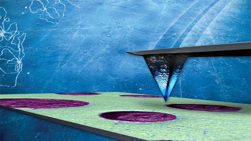
Some of the most progressive studies in nanotechnology require the precise fabrication and interconnection of nanometer-scale structures. Anodic oxidation nanolithography uses an applied voltage to the AFM probe to create an oxide layer directly under the tip. Since the oxide only forms under the tip, very narrow oxide lines can be written on the sample.

Bruker’s NanoMan and NanoPlot software packages provide a user-friendly interface for high-definition nanolithography with a variety of "writing" techniques, in either a graphical point-and-click mode, or in a recipe-driven mode. Lithography is also possible on the Dimension Icon® system using Piezoresponse Force Microscopy (PFM).

Anodic oxidation on Si using SCM-PIT tip to create a nanolithography pumpkin. 5μm scan size showing Height data with shadowing.
Input value is invalid.

Get instant access to the full-length AFM modes handbook.

The Definitive AFM Modes Handbook contains everything you need to understand, select, and apply AFM techniques in materials research, including:

  • An easy-to-use framework for understanding the seven categories of AFM modes, their capabilities, and their core uses
  • Detailed descriptions of 50+ modes and variants (including 300+ data images)
  • Summary information about what each mode is, how it works, and when to use it
  • Our experts' top probe recommendations for each mode
Please enter your first name
Please enter your last name
Please enter your e-mail address
Please enter a valid phone number
Please enter your Company/Institution
What best describes your current interest?
Please accept the Terms and Conditions

             Privacy Notice   Terms of Use


  * Please fill out the required fields.

Your download is now available.


Note:
If you exit this page, you may not be able to reopen this download window without re-submitting the form.