Application of Atomic Force Microscopy in the Study of Semiconductor Materials and Devices
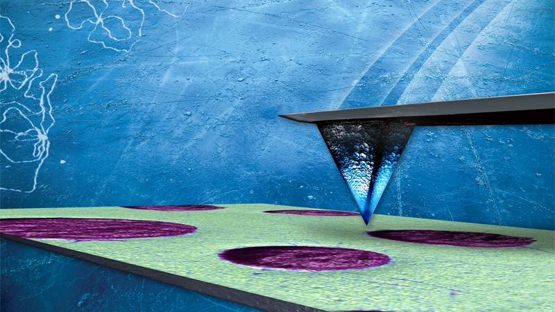
Discover how Atomic Force Microscopy (AFM) is used in semiconductor research and development for the nanoscale characterization of topographic, electrical, mechanical, and chemical properties.
- [00:00:01] Welcome and review of the Bruker AFM product catalog.
- [00:05:00] Introduction to AFM-based semiconductor research, including topography and morphology imaging and 3D metrology.
- [00:14:30] Case studies of the practical uses of AFM in semiconductor reseach, including its use in failure analysis of devices.
- [00:40:00] Overview of additional properties made available by Bruker's AFM instrumentation, including electrical, mechanical, and chemical characterization at nanometer-scale resolution.
- [00:55:00] Live question and answer session with the presenters.