FilmTek 3000 PAR-SE
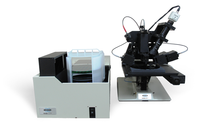

FilmTek 3000 PAR-SE
The FilmTek™ 3000 PAR-SE is one of our most advanced and versatile metrology solutions, able to meet extremely challenging measurement demands in both R&D and production environments. Though it achieves idustry-leading accuracy and precision in nearly any advanced thin film measurement application, this system excels at material characterization of product wafers and patterned films on both transparent and non-transparent substrates.
Like our other PAR-SE products, this system combines rotating compenstor-based spectroscopic ellipsometry, DUV multi-angle polarized reflectometry, our patented parabolic mirror micro-spot optical design, our proprietary Multi-Angle Differential Polarimetry (MADP) and Differential Power Spectral Density (DPSD) technology, and our advanced material modeling software and optimization algorithms. It is also uniquely capable of spectroscopic transmission measurements across an extended spectral range. As a result, FilmTek 3000 PAR-SE not only achieves industry-leading sensitivity to changes in ultra-thin films and multilayers, but is also uniquely well suited for use with absorbing patterned films or product wafers containing absorbing structures.
Additionally, the FilmTek 3000 PAR-SE's hardware and software can both be easily modified to satisfy unique customer needs and measurement requirements far outside those of mainstream film metrology applications, including those requiring generalized ellipsometry or more advanced automation.
Measurement Capabilities
Enables simultaneous determination of:
- Multiple layer thicknesses
- Indices of refraction [ n(λ) ]
- Extinction (absorption) coefficients [ k(λ) ]
- Energy band gap [ Eg ]
- Composition (e.g., %Ge in SiGex; % Ga in GaxIn1-xAs; %Al in AlxGa1-xAs etc.)
- Surface roughness
- Constituent, void fraction
- Crystallinity/Amorphization (e.g., of Poly-Si or GeSbTe films)
- Film gradient
System Components
Standard:
- Spectroscopic reflection measurement
- Spectroscopic transmission measurement
- Spectroscopic ellipsometry with rotating compensator design (295nm-1700nm)
- Multi-angle, polarized spectroscopic reflection (190nm-1700nm)
- Spectroscopic transmission measurement (220nm-1000nm)
- Measures film thickness and index of refraction independently
- Multi-Angle Differential Polarimetry (MADP) technology with SCI’s patented Differential Power Spectral Density (DPSD) technology
- Ideal for measuring ultra-thin films (0.03 Å repeatability on native oxide)
- Camera for imaging measurement location
- Pattern recognition
- 50 micron spot size
- Advanced material modeling software
- Bruker's generalized material model with advanced global optimization algorithms
Optional:
- Automated sample handling
- Generalized ellipsometry (4×4 matrix generalization method) for anisotropy measurements (nx, ny, nz)
- SECS/GEM
Typical Application Areas
Virtually all translucent films ranging in thickness from less than 100 Å to approximately 150 µm can be measured with high precision. Typical application areas include:
- Photonics and telecom
- Flat panel display
With flexible software that can be easily modified to satisfy unique customer requirements in R&D and production environments.
Technical Specifications
| Film Thickness Range | 0 Å to 150 µm |
|---|---|
| Film Thickness Accuracy | ±1.0 Å for NIST traceable standard oxide 100 Å to 1 µm |
| Spectral Range | 190 nm - 1700 nm (220 nm - 1000 nm is standard) |
| Measurement Spot Size | 25 µm - 300 µm (50 µm standard); 2 mm (70°) |
| Spectral Resolution | 0.3 - 2 nm |
| Light Source | Regulated deuterium-halogen lamp (2,000 hrs lifetime) |
| Detector Type | 2048 pixel Sony linear CCD array / 512 pixel cooled Hamamatsu InGaAs CCD array (NIR) |
| Computer | Multi-core processor with Windows™ 10 Operating System |
| Measurement Time | ~2 sec per site (e.g., oxide film) |
Performance
| Film(s) | Thickness | Measured Parameters | Precision (1σ) |
|---|---|---|---|
| Oxide / Si | 0 - 1,000 Å | t | 0.03 Å |
| 1,000 - 500,000 Å | t | 0.005% | |
| 1,000 Å | t , n | 0.2 Å / 0.0001 | |
| 15,000 Å | t , n | 0.5 Å / 0.0001 | |
| 150,000 Å | t , n | 1.5 Å / 0.00001 | |
| Photoresist / Si | 200 - 10,000 Å | t | 0.02% |
| 500 - 10,000 Å | t , n | 0.05% / 0.0002 | |
| Nitride / Si | 200 - 10,000 Å | t | 0.02% |
| 500 - 10,000 Å | t , n | 0.05% / 0.0005 | |
| Polysilicon / Oxide / Si | 200 - 10,000 Å | t(POLY) , t(OXIDE) | 0.2 Å / 0.1 Å |
| 500 - 10,000 Å | t(POLY) , t(OXIDE) | 0.2 Å / 0.0005 |