X-ray Defect Inspection

X200

Improve process control systems with precise, real-time metrology and defect feedback

High-resolution automated in-line X-ray inspection system

The X200 X-ray Imaging (XRI) system is on the leading edge of a new category of in-line transmissive inspection and metrology equipment. This one-of-a-kind, no-compromises platform for advanced packaging provides fully automatic 100% inspection and real-time feedback on the die-attach process.

As such, the high-speed, high-resolution X200 is the ideal defect inspection and production metrology solution for a wide range of semiconductor applications, from system-in-package (SiP) to 2.5D/3D integrated circuit (IC) integration.

X200

With the X200 system, Bruker has optimized X-ray imaging to make full defect inspection feasible in-line on the manufacturing floor. Instead of pulling a small sample from the line for lengthy and data-limited 3D X-ray and cross-sectioning, 100% of production can be automatically monitored in real-time for maximal quality, reliability, and production yield.

Real-time
defect inspection
Delivers high-resolution data over a large field-of-view in seconds to enable 100% sampling strategies.
Full-wafer
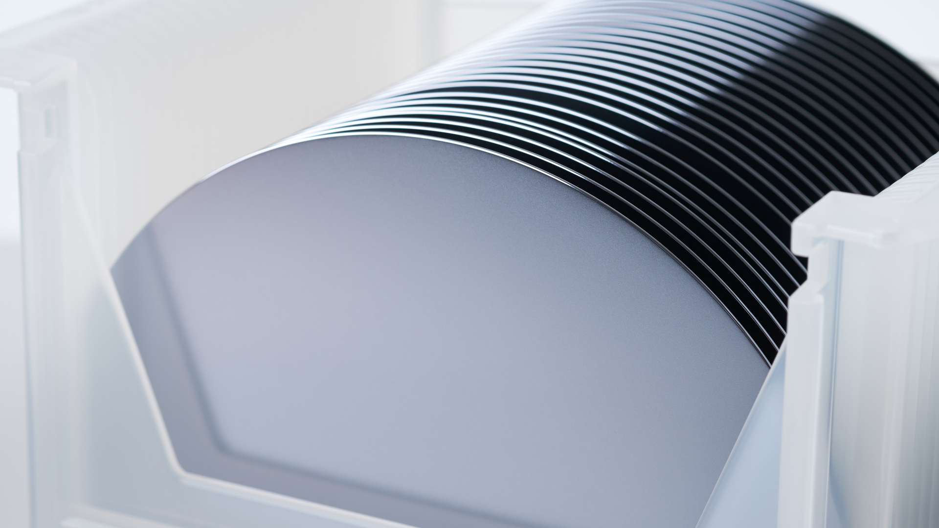
inspection earlier in the process step

Enables new levels of quality, reliability, and production yield.


Accurate
latent defect sensitivity 
Reveals the marginal defects that can pass electrical testing.
Features

X-ray Defect Inspection Redefined

X200 is a one-of-its-kind solution. Its specialized design features Bruker-exclusive technology, such as our proprietary source-detector-sample architecture and proprietary transmissive architecture (with 1000 W source and high-resolution 30MP, 16-bit camera).

This unique design gives X200 a unique set of capabilities, including:

  • Wide field of view of 12 mm x 18 mm
  • High resolution of 2.8 µm/pixel
  • High throughput of 1-2 full 300 mm wafers inspected per hour
  • Inference of 3D structural information based on high-resolution 2D grayscale data

Specialized Time- and Cost-Saving Design

X200 is specifically designed to increase efficiency and cost-effectiveness in both the measurement and analysis stages.

Faster, More Accurate Measurements

X200 is uniquely able to achieve full wafer surface scanning -- at high speed without any sacrifice of resolution. This enables a high through put,  high accuracy 100% sampling strategy, thereby saving time during the measurement stage.

Automated, Comprehensive Analysis

The X200 Data Analysis Toolkit completely eliminates the need for manual processing and interpretation of X-ray images. Its computer vision algorithms locate and analyze features of interest. Machine learning performs automatic defect classification and optimizes the pass/fail criteria to meet unique application specifications.

X200’s Data Analysis Toolkit provides:

  • Comprehensive bump metrology and defect inspection algorithms
  • Automated feedback on critical attributes (e.g., solder joint quality, voids, bridges, and extra/missing solder)
  • Straightforward recipe setup with pre-configured data processing and reporting options
  • On-tool data visualization for process trends and defect review
X200 can measure bump height, a predictive indicator of wetting behavior. This requires no cross-sectional or high-resolution defect imaging beyond initial validation step.
Applications

Perfected Inspection and Metrology

Semiconductor applications require ever tighter tolerances, smaller interconnects, and more vertical layers. X200 was developed to quickly and precisely identify small changes in device interconnect structures and to provide real-time feedback for process control and screening.

X200 is enabling semiconductor manufacturers to radically increase quality, reliability, and productivity.

Case Study 1

Advanced Processors

Non-wet detection is vital to ensuring functionality of advanced processors.

In this example, X200 analysis showed both warpage and tilt contribute to a non-wet failure mode. When compared to manual X-ray inspection, X200 achieved 100% accuracy and additionally flagged non-wet parts missed by operators.

Case Study 2

Automotive Microcontrollers

Improper wetting leads to critical safety concerns for automotive microcontrollers.

In this example, X200 analysis showed that both warpage and tilt contribute to a non-wet failure mode. On ~300 microcontroller parts, X200 achieved 100% accuracy for non-wet detection and a precision-to-tolerance ratio <10%.

Case Study 3

Wireless Chips

High-throughput and high-accuracy detection of non-wet defects is important for wireless chips.

In this example, the machine learning algorithms integrated into the X200 software helped to establish a fast and accurate process for non-wet detection using automatic defect classification (ADC). Using the X200 workflow, 100% of parts were accurately labeled as pass or fail based on non-wet defects, even including a non-wet part that was missed by manual X-ray labeling.


Contact us to discuss your specific process needs and measurement requirements.

More Information

Frequently Asked Questions

Why is it important to have a high-sampling rate for metrology in advanced packaging?

With increasing bump densities and demand for defect rates <100 ppb, it is critical to provide active feedback control on the die-attach process to minimize variations. By adopting a 100% sampling rate strategy, one can dramatically decrease the time it takes to discover an excursion from weeks to a couple days.

What makes X200 different from other X-ray tools?

X200 utilizes a unique, patented architecture optimized for high-speed inspection, which makes it 10 to 100 times faster than other X-ray tools for the same measurement capability. With advanced computer vision and AI, the process issues and defects are reported automatically.

Does X200 also help in R&D?

Typical learning cycles in R&D depend on failure analysis labs, which take days to identify failures on a few parts. With X200, every part on the wafer can be analyzed within an hour to provide rich insights on the process issues. By reducing the learning cycle time, one can achieve faster time-to-market and maximize productivity over the product lifetime.

How do I determine if my process requires X200 inspection?

This depends on a variety of factors, including device complexity and cost of defects. Some possible considerations include:

  • 1000+ bumps and <80um bump diameter
  • Die-attach placement accuracy <10um
  • Cost of final device >$100

Contact us to learn more about successful use-cases and suitable applications.

Support

How Can We Help?

Bruker partners with our customers to solve real-world application issues. We develop next-generation technologies and help customers select the right system and accessories. This partnership continues through training and extended service, long after the tools are sold.

Our highly trained team of support engineers, application scientists and subject-matter experts are wholly dedicated to maximizing your productivity with system service and upgrades, as well as application support and training.
Contact Us

Input value is invalid.

* Please fill out the mandatory fields.

Please enter your first name
Please enter your last name
Please enter your e-mail address
Please enter your Company/Institution


Please enter a valid phone number

ⓘ Used to provide a faster response to your request/question.

Please enter a valid phone number

ⓘ Used to provide a faster response to your request/question.

Please enter a valid phone number

ⓘ Used to provide a faster response to your request/question.

Please enter a valid phone number

ⓘ Used to provide a faster response to your request/question.

Please add me to your email subscription list so I can receive webinar invitations, product announcements and events near me.
Please accept the Terms and Conditions

             Privacy Notice   Terms of Use