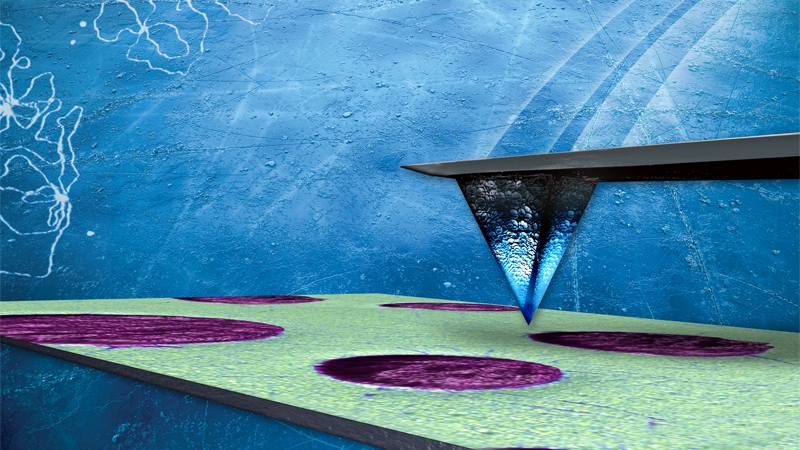
Conductive AFM (C-AFM)
Researchers map variations of electrical conductivity for a range of studies and processes, including electrical defect characterization and investigation of conductive polymers, semiconductors, nanotubes, and even certain organic materials.
Conductive AFM (C-AFM), and the related modes Tunneling AFM (TUNA) and PeakForce TUNA™, are powerful current-sensing techniques that represent part of Bruker’s array of nanoelectrical characterization modes.
C-AFM is a secondary imaging mode derived from Contact Mode that characterizes conductivity variations across medium- to low-conducting and semiconducting materials. It is used to measure and map current in the 2pA to 1µA range while simultaneously collecting topographic information.
With the help of Conductive Atomic Force Microscopy (C-AFM) analysis in the PeakForce Tunneling AFM (PeakForce TUNA) module of the MultiMode 8, we were able to understand the location-specific nanoscale electrical conductivity of doped semiconductors. This has led us to explore many new materials and their electronic properties at nanoscale. We have been using the MultiMode 8 for the past three years and I must say this instrument is really powerful and robust.
Dr. Emila Panda, Indian Institute of Technology (IIT) Gandhinagar, India


