What is EBSD? An Introduction to Electron Backscatter Diffraction
EBSD (Electron Backscatter Diffraction) is a powerful technique for the analysis of the crystallographic orientation and microstructure of crystalline materials down to the nanoscale.
EBSD is a Scanning Electron Microscope (SEM)-based technique that allows users to correlate local crystal orientation with a sample's microstructure. This makes it a valuable tool for researchers and engineers who wish to understand the relationship between the properties of crystalline materials and their internal structure.
This insight into a cruical relationship is what makes EBSD a popular technique for anyone developing advanced materials. By developing understanding of the relationship between microstructural properties and macroscopic behavior engineers can refinine processing methods to favour certain properties. EBSD therefore facilitates the production of components and materials that exhibit optimum performance and behavior for their application.

Figure 1. Diagram illustrating how the inter-relationship between the properties, processing and structure of a material influence a material's performance. Characterization is at the heart of these four factors.
How Does EBSD Work?
Electron Backscatter Diffraction is a SEM-based technique that measures the interaction between the electron beam of the SEM with a sample's atomic structure.
The EBSD measurement process can be broken down into the following steps:
1 - The Backscattering of Electrons
A focused electron beam is directed onto the surface of a sample. The high-energy electrons interact with the atoms in the sample, leading to various electron scattering phenomena.
Some of the electrons are backscattered off the sample due to interactions that happen in the top few nanometers below the sample surface. To increase scattering yield, the sample is tilted by approximately 20 degrees compared to the beam. For this reason EBSD measurements are mostly carried out using this sample orientation.
The energy and direction of the backscattered electrons are related to the local arrangement of atoms in the sample, i.e. the crystallographic orientation and phase.
Video 1: A video depicting the functioning principle of EBSD technique
2 - Pattern Formation, Detection & Mapping
A small fraction of the backscattered electrons form a diffraction pattern a.k.a. Electron BackScatter Pattern (EBSP) on a phosphor screen or a semiconductor sensor placed in front of the tilted sample. This pattern, also known as a Kikuchi pattern, contains information about the crystallographic orientation and phase present at that location on the sample.
A camera inside the EBSD detector captures the diffraction pattern and transfers it to a computer for analysis. The camera is synchronized with the electron beam movement and can capture thousands of images/patterns per second. The electron beam is automatically moved to collect patterns from a grid of points across the sample surface.

Figure 2. A crystal lattice for Tri-Chronium Silicide (Cr3Si) with the Kikuchi pattern formed by the interaction of the electron beam with this structure.
3 - Data Analysis
The collected EBSPs are then analyzed to determine the crystallographic orientation of each measurement point across the grid. This information is used to create a detailed map of the sample's crystallographic features, including grain boundaries, grain orientations, and other microstructural characteristics.

Figure 3. Typical EBSD map showing local crystal orientation distribution using a standard IPF coloring scheme.
What is Microstructure?
The microstructure of a material refers to its internal structure at the microscopic level, including the arrangement of its atoms, crystals/grains, phases, and defects.
Understanding the microstructure and, its evolution under certain conditions, is crucial in materials science and engineering because it greatly influences the mechanical, thermal, electrical, and other properties of a material, as well as how these properties evolve during a component or material's lifetime of a component.

Figure 4. Color coded ForeScatter Electron image depicting the complex microstructure of a SiC sample from nuclear applications. The color contrast indicates that the various features have different crystal orientations but it does not indicate the actual crystal orientation. For such quantitative type of information, one needs to acquire an EBSD map.
What Applications is EBSD Used For?
Electron Backscatter Diffraction (EBSD) is widely applied for the analysis of crystalline materials across a wide range of fields, some of the most common include:
Material Science and Metallurgy
Grain Orientation Mapping: EBSD is commonly used to determine the orientation, size and shape distribution of grains in crystalline materials. This information is crucial for understanding the mechanical and thermal properties of metals and alloys.
Phase Identification & Distribution: EBSD can be used to identify different phases in a material, helping researchers understand the microstructural evolution during processes like heat treatment.
Texture Analysis: By analyzing the crystallographic texture of a material, researchers can gain insights into preferred orientations of grains, which is essential in predicting material properties or estimating the lifetime of a component.

Figure 5. Phase distribution map of a duplex steel showing Ferrite (red) and Austenite (green) phases.
Semiconductors and Electronics
Research & Development: EBSD can be used to analyze grain size and crystal orientation distributions and even identification and distribution analysis of polymorph phases like those present in ferroelectric materials which are the cornerstone of the next generation memory devices.
Failure Analysis: When electronic devices fail, EBSD can be used to investigate the root causes by examining the crystallographic structure of the materials involved. EBSD can also be used to investigate the formation of deleterious intermetallic phases in lead free solders.

Figure 6. Orientation contrast image taken of a gold-based electrical connection on a microelectronic device.
Thin Film Characterization
Thin Film Quality Assessment: EBSD can be used to characterize the crystallographic quality of thin films or the grain size distribution which are crucial parameters in electronic, optical and semiconductor applications.

Figure 7. Grain orientation distribution map of a 20 nm gold film on a 5 nm Si3N4 membrane. This map was captured using Transmission Kikuchi Diffraction (TKD).
Geology
Mineral Identification: EBSD can be employed to identify minerals in rocks based on their crystallographic characteristics. This is valuable for understanding the geological history and conditions of a region.
Deformation Studies: Studying the crystallographic orientation of minerals helps in understanding the deformation history of geological materials.

Figure 8. An EBSD phase distribution map of a marine rock (oceanic gabbro) sample, showing the presence & distribution of 10 different phases as well as eroded regions & pores.
Biology and Biomaterials:
Biomineralization Studies: EBSD can be used to study the crystallography of biominerals, providing insights into the formation of biological materials like bones and teeth.
Implant Materials: Understanding the crystallographic properties of biomaterials and implants helps in designing materials with better biocompatibility and longer lifetime.

Figure 9. Orientation map from an Ostrich eggshell showing large columnar grains with a strong preference for orientations with c-axis perpendicular to the egg surface.
What Type of Detector Should You Use for EBSD?
There are two major aspects that need to be considered when choosing an EBSD detector: technical and commercial performance.
Technical performance is driven by the specific requirements of the envisioned application(s), and includes the spatial resolution, the speed, the signal efficiency, the sensor pixel resolution, etc.
The commercial aspect reflects the cost of initial investment, cost of ownership and down time. The latter two factors are heavily influenced by the detector reliability or failure rate and when a detector does fail, how quickly can the detector be operational again?
Currently there are two main types of EBSD detectors:
Scintillator-Based EBSD Detectors
Scintillator-based detectors use a phosphor screen to convert backscattered electrons into visible light.
The patterns of light produced on the phosphor screen are then detected by a charge-coupled device (CCD) or Complementary Metal-Oxide-Semiconductor (CMOS) camera. Most commercially available EBSD detectors today are scintillation-based detectors and cover the entire spectrum of EBSD applications.

Figure 10. An eFlash FS EBSD detector - Kikuchi patterns are captured on the flat phosphor screen of the detector head.
Direct Electron Detectors (DED)
As the name implies, Direct Electron Detectors capture the backscattered electron signal directly using a semiconductor material as an active surface, which is coupled to a chip behind it.
Direct electron detection offers improved sensitivity compared to scintillator-based detection which could benefit future detectors designed for ultra-high speed EBSD and low-kV EBSD applications.
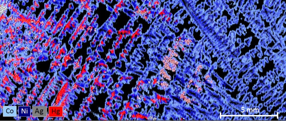
Combining Microstructural & Elemental Analysis
Researchers working with Electron Backscatter Diffraction often want to know not only the orientation and structure of grains and phases within their sample but also their chemical composition. This is where EDS-EBSD, ie. EBSD combined with Energy Dispersive Spectroscopy (EDS), is particulary useful. EDS is a complementary SEM-based technique for the elemental mapping of samples.
The combination of EBSD and EDS provides a powerful analytical approach which can be used to understand the structure-property relationships in materials, which is essential for various fields of materials science like metallurgy and semiconductor research. Combined EBSD & EDS is also a popular tool among geoscientists working with little known samples containing multiple phases.

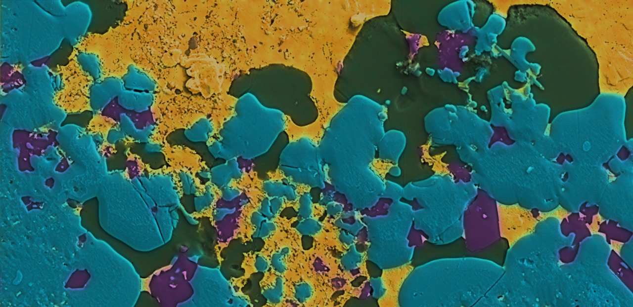
Figure 11. EBSD phase map of a thermal barrier coating on a Ni superalloy sample. EDS data was used to separate automatically two carbide phases which create very similar Kikuchi patterns.


Augmenting EBSD with More Analytical Capabilities
In addition to systems for EBSD Bruker Nano Analytics provides additional systems to add even more analytical capabilities to electron microscopes.
Our Electron Microscope Analyzer range includes systems for:
- EDS (Energy Dispersive Spectroscopy) - for elemental analysis and mapping
- Micro-XRF on SEM - for trace element detection and layer analysis
- WDS (Wavelength Dispersive Spectroscopy) - for elemental mapping with increased analytical precision

Figure 12: The Electron Microscope Analyzer range includes systems for EDS, EBSD, WDS and micro-XRF on SEM.